Home » Component data » Transistor data » this page
2N2369 & 2N2369A Transistors Data
Key transistor data for the 2N2369 & 2N2369A switching transistors including key electrical parameters, pinout, package type and many other key transistor details.
There are very few electronic components that have earned as legendary a status as the 2N2369 and its later version the 2N2369A have. Its switching speed was legendary for its time, and even now it is a 'goto' device for many,
The 2N2369 was originally developed to solve the critical "storage time" delays that plagued early digital systems, and as a result this device became the gold standard for nanosecond-level pulse manipulation.
Although t was introduced in the 1960s, the later version of the device, the 2N2369A is still widely used and can be obtained from many electronic component distributors with ease.
Although, not was widely manufactured as the 2N2222, the 2N2369 and the 2N2369A could be classed as 'jelly bean' components because they have been available for many years, they are manufactured by many companies, they are cheap and they are in very many designs.
Key details and performance parameters for the 2N2369 & 2N2369A switching transistors.
| Transistor parameters & data |
|
|---|---|
| Parameters | Details |
| Transistor type | NPN silicon switching transistor |
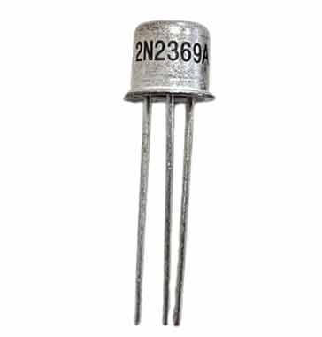
| Package type | TO18 |
| VCBO max (V) | 40 |
| VCEO max (V) | 15 |
| VEBOmax (V) | 4 |
| IC max (mA) | 500 |
| TJ Max °C | 175 |
| PTOT nW | 360 |
| fT min (MHz) | 500 |
| COB | 4p |
| hfe | 40 min |
| IC for hfe | 10 mA |
| Similar / equivalents | BSX20 |
Outline:
![]()
Pinout:
![]()
Notes: Switching transistor which is ideal for many general purpose applications and works well, even for some RF applications if nothing else is available.
Explanation of transistor parameters
| Parameter | Explanation |
|---|---|
| VCBO Max | Maximum collector-base voltage with emitter open circuit . |
| VCEO Max | Maximum collector-emitter voltage with base open circuit. |
| VEBO Max | Maximum emitter-base voltage with collector open circuit. |
| VCEsat (included where applicable) | The voltage drop across the collector-emitter when the transistor is fully saturated (acting as a closed switch). |
| IC Max | Maximum collector current. |
| Parameter | Explanation |
|---|---|
| TJ | Maximum junction temperature. |
| PTOT Max | Maximum device dissipation normally in free air at 25°C unless other conditions indicated. |
| fT Min | Minimum cutoff frequency at which the current gain in a common emitter circuit falls to unity. |
| COB Max | Maximum collector capacitane, normally measured with emitter open circuit. |
| hFE | DC current gain for HFE at IC. [Note hfe is the small signal gain and although this may be slightly different, the transistor current gain will vary considerably from ne transistor to the next of the same type.] |
| PTOT Max | Maximum device dissipation normally in free air at 25°C unless other conditions indicated. |
These are the main transistor parameters that have been included in our list. There are others, but these help quantify the main elements of the performance of the transistor.
Please note, that the data given is the best estimate we can give within a tabulated summary of this nature. Parameters also vary between manufacturers. Electronics Notes cannot accept any responsibility for errors, inaccuracies, etc, although we do endevaour to ensure the data is as accurate as possible.
Notes and supplementary information
• Availability & sources
The 2N2369A is available from a number of stockists and electronic component distributors many of which are given in the table below.
2N2369A Component Distributor, Stock and Pricing
• Additional details
The 2N2369 and 2N2369A are switching transistors which are ideal for many applications and they work well, even for some RF applications, although it's best to use a proper RF transistor for this.
• 2N2369 development and history
The 2N2369 is one of the most famous and enduring NPN silicon switching transistors in electronics history.
The 2N2369 was developed during the mid-1960s, which was a period defined by the rapid expansion of early digital computing and high-speed pulse applications. The 2N2369 was designed specifically to minimize storage time - the delay that occurs when a transistor attempts to switch from a saturated "ON" state to its "OFF" state.
By optimizing the base-emitter and collector-base junctions for extremely low carrier lifetime, the engineering team created a device that could switch in nanoseconds, making it an essential component for the logic gates and pulse-shapers of that era.
The architecture of the 2N2369 relied on sophisticated planar manufacturing techniques, which were state-of-the-art at the time. This process allowed for highly precise control over the doping profiles of the silicon die, ensuring the device could maintain its rapid switching capabilities while remaining stable under varying electrical loads.
The 2N2369 was encased in a miniature TO-18 metal can, and the structure was built for durability and thermal efficiency, allowing it to perform reliably in the high-density, air-cooled environments common in the mainframe computer chassis of the 1960s.
Its impact on the electronics industry was profound, as it essentially became the "go-to" transistor for high-speed digital switching circuits for decades. By providing a reliable, low-cost solution that significantly outperformed general-purpose transistors in pulse-width and high-frequency applications, the 2N2369 allowed engineers to push the clock speeds of digital systems further than previously possible. Even today, while modern integrated circuits have largely replaced discrete logic, the 2N2369 remains a celebrated classic for engineers exploring analog pulse circuits and fast signal switching.
• 2N2369A introduction & rationale
While the original 2N2369 was a ground-breaking component for low-voltage logic circuits, its 15V breakdown limit proved too restrictive for many emerging industrial and communication applications that required higher signal swings or greater safety margins.
The primary reason behind the introduction of the A-suffix version was the need for increased reliability and versatility.
Engineers found that the standard 2N2369 was highly susceptible to voltage transients because its collector-emitter breakdown voltage drops sharply to a low 15V if the base is left open or weakly driven (VCEO). By refining the diffusion process and reducing leakage currents, manufacturers created the 2N2369A.
This improved version guaranteed a much sturdier 40V breakdown rating when the base is firmly shorted or clamped to the emitter (VCES).
This refinement allowed the device to safely handle voltage spikes in high-speed switching environments—such as high-voltage pulse drivers and robust industrial controllers—without risking thermal runaway or sacrificing its legendary switching speed.
Beyond the voltage boost, the 2N2369A was introduced to address the demand for tighter performance consistency. As mass-production techniques matured, the "A" classification allowed manufacturers to bin components that met higher standards for gain, leakage current, and switching stability. This effectively gave designers a "premium" version of a known reliable component.
By providing a part that was drop-in compatible but significantly more robust, the industry ensured the 2N2369 architecture could continue to thrive in more challenging environments, effectively extending the lifespan of that specific design family for several decades.
• The golden secret
One fascinating fact about the 2N2369 / 2N2369A was a special ingredient that was used int he doping of thee transistors and it was part of the reason for their speed.
The reason for its incredible speed wasn't just physical geometry; it was chemistry. Manufacturers literally introduced microscopic amounts of gold into the silicon lattice during the diffusion process.
This gold acted as a recombination centre for charge carriers. By forcing the "holes" and "electrons" to recombine faster, the gold quenches the transistor turn off delay time, allowing it to shut off with unmatched speed.
It is a brilliant example of early semiconductor physics — using a precious metal to significantly improve the performance of the device, enhancing it well above anything else at the time.
But today, gold is avoided in mainstream semiconductor fabrication. In standard MOSFETs (found in CPUs), gold acts as an impurity that increases leakage current and degrades carrier mobility.
It is also a significant contamination hazard - it is considered a "killer" contaminant in modern silicon fabs. It diffuses rapidly, and stray gold atoms can ruin standard transistors, necessitating extremely strict isolation.
• Silicon structure and manufacture
The 2N2369 transistor uses an epitaxial process in its manufacture and this enables the right level of precision to be contained for the doping profiles to be achieved.
The epitaxial process consists of a thin, high-purity layer of single-crystal silicon which is grown on top of the heavily doped substrate. Gold doping is typically used as mentioned above to enable the required speeds to be obtained.
This allows the 2N2369 to have a very low collector-base capacitance and a tightly controlled doping profile, which directly enables its nanosecond-level turn-on and turn-off times.
The internal silicon cross-section is structured in distinct layers, engineered to reduce charge storage and minimize switching times:
Top Metal Contacts: Aluminum traces connect directly to the emitter and base regions for wire-bonding to the external package pins.
N+ Emitter Layer: Heavily doped N-type silicon injected at the top surface; allows for high current gain and rapid electron injection.
P- Type Base Region: A very thin layer of P-type silicon that acts as a control gate; kept incredibly narrow to minimize transit time and storage time.
N- Epitaxial Collector Layer: A lightly doped layer of N-type silicon grown over the collector substrate; provides high breakdown voltage and low capacitance.
N+ Substrate: A heavily doped base layer at the bottom providing low-resistance electron flow to the collector pin.
Bottom Metal Contact: Gold or alloy back-metallization connects the bottom substrate to the TO-18 metal case (acting as the collector).
Silicon Dioxide SiO2 Layer: Covers the top of the silicon die to protect the junctions from contamination and environmental damage (the "planar" characteristic).
Transistor profile summary:
| Region | Doping Level | Material Type | Function |
|---|---|---|---|
| Emitter | Heavily Doped (N+) | Silicon | Injects electrons into the base. |
| Base | Lightly Doped (P) | Silicon | Controls current flow. |
| Collector | Moderately Doped (N-) | Silicon | Collects electrons from the emitter/base. |
• Radiation hardened performance
The 2N2369 / 2N2369A were really important in the 'Cold-War' era as a result of their radiation hardened performance.
Because of their specific internal structure and planar manufacturing, the 2N2369 family was surprisingly resilient to certain types of environmental stress, and notably radiation, compared to other devices of the time.
This made them a favourite device for military and aerospace applications in the 1970s and 80s.
When engineers needed a fast, reliable switch that wouldn't fail the moment it was exposed to the harsh conditions of a satellite or a field-deployed radar system, they reached for the 2N2369.
 Written by Ian Poole .
Experienced electronics engineer and author.
Return to Component Data menu . . .