Automated X-Ray Inspection AXI for PCB & BGA
Key essentials about automated X-ray inspection, AXI, systems used for inspection PCB printed circuit board assemblies and especially ones with BGA ICs.
Automatic Test Equipment, ATE Includes:
PCB inspection techniques
Automated optical inspection, AOI
Automated X-ray inspection, AXI
Design for AOI test
See also:
ATE basics
In-Circuit test, ICT
Functional test, FATE
Developing test strategy
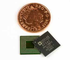
Automatic optical inspection works very well in electronics manufacturing for printed circuit boards where joints are visible. However many PCBs today are using technologies such as ball grid array, BGA integrated circuits and chip scale packages, CSPs where the solder connections are not visible. This has arisen as a result of the need for greater numbers of interconnections to integrated circuit packages and as a general result of increasing complexity. In these and many other instances it is necessary to carry out checks using automated X-Ray inspection, AXI, equipment that can not only check the solder joints under components, but also reveal many defects in solder joints that may not be visible with ordinary optical inspection equipment.
In recent years, the need for automated X-Ray inspection equipment has grown considerably and as a result, a much wider range of equipment is available. Additionally the techniques used in automated X-Ray inspection equipment has improved and this has enabled far greater levels of detection to be achieved for printed circuit board, PCB manufacture.
As one significant improvement in AXI, automated X-ray inspection, not only are 2D or two dimensional techniques available, but machines utilising 3D technology are available and give significant improvements in performance.
AXI technology features
AXI, automated X-ray inspection systems are able to monitor a variety of aspects of a printed circuit board assembly production. They would normally be placed after the solder process to monitor defects in PCBs after leaving the soldering process. They have the distinct advantage over optical systems that they are able to "see" solder joints that are under packages such as BGAs, CSPs and flip chips where the solder joints are hidden.

AXI, automated X-ray inspection systems are not only able to "see" through the chips, but they are also able to provide an internal view of the solder joints. In this way they are able to detect voiding within a solder joint that may otherwise look perfectly acceptable.
This means that AXI, automated X-ray inspection systems are able to provide additional information over that which could be provided by purely optical systems to ensure that solder joints are being made to the required standard.
AXI, automated optical inspection can inspect the features of solder joints providing information on the way the soldering process is operating. Parameters such as solder thickness, joint sizes and profiles can be undertaken on specific joints on boards. These can then be used to provide data on the solder process and how well it is operating. AXI systems are also able to see the heel of the joint which AOI systems are unable to see as they are masked by the leads from the ICs as shown.

When an automated X-ray inspection system, or an optical system is used within an electronics PCB manufacturing process, the defects and other information detected by the inspection system can be quickly analysed and the process altered to reduce the defects and improve the quality of the process. In this way not only are actual faults detected, but the process can be altered to reduce the fault levels on the boards coming through. Accordingly they ensure that the highest standards are maintained and they are particularly useful when new boards are being set up and the process needs to be optimised.
It should be realised that AXI is only one of the number of tools that can be used within an electronics PCB manufacturing organisation. Two other tools, namely AOI, automatic optical inspection, and ICT, in-circuit test can provide similar information in many areas. The table below provides a comparison of the different types on information that each form of automatic test equipment, ATE can provide. Decisions about which type of types of testing should be used can then be made.
| Comparison of the major defect detection capabilities of AOI, AXI and ICT | |||
|---|---|---|---|
| Defect type | AOI | AXI | ICT |
| Soldering defects | |||
| Open circuits | Y | Y | Y |
| Solder bridges | Y | Y | Y |
| Solder shorts | Y | Y | Y |
| Insufficient solder | Y (not heel of joint) | Y | N |
| Solder void | N | Y | N |
| Excess solder | Y | Y | N |
| Solder quality | N | Y | N |
| Component defects | |||
| Lifted lead | Y | Y | Y |
| Missing component | Y | Y | Y |
| Misaligned or misplaced component | Y | Y | Y |
| Incorrect component value | N | N | Y |
| Faulty component | N | N | Y |
| BGA and CSP defects | |||
| BGA shorts | N | Y | Y |
| BGA open circuit connections | N | Y | Y |
Automated X-ray inspection, AXI has an important place in many electronics PCB manufacturing organisations. AXI is able to provide a fast and in-depth and accurate inspection of PCBs passing through the production facility and in this way provide real-time feedback that enables the production system to be optimised to enable high quality reliable circuits to be produced. Although more expensive than some other forms of inspection, AXI has many advantages and these need to be carefully balanced against the costs to ensure whatever choice is made, it is correct for the particular production environment.
 Written by Ian Poole .
Experienced electronics engineer and author.
More Test Topics:
Data network analyzer
Digital Multimeter
Frequency counter
Oscilloscope
Signal generators
Spectrum analyzer
LCR meter
Dip meter, GDO
Logic analyzer
RF power meter
RF signal generator
Logic probe
PAT testing & testers
Time domain reflectometer
Vector network analyzer
PXI
GPIB
Boundary scan / JTAG
Data acquisition
Return to Test menu . . .


