Home » Component data » Transistor data » this page
2N2222 & 2N2222A Transistor Data
Key data & information about the 2N2222 & 2N2222A transistors including key electrical parameters, information about its technology, development story & the people involved.
The 2N2222 transistor is a very popular transistor that has been available for many years.
It is an ideal general purpose transistor for both analogue and switching applications and it can handle a good amount of current and exhibits a low VCE(sat).
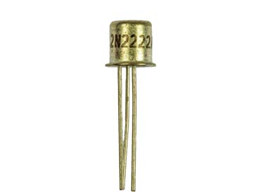
Although it has been available for very many years, it is still a good choice for many circuits. It is often referred to as a jelly-bean device because it has been around forever, its available from a wide variety of manufacturers and suppliers and it is very cheap . . . and of course it performs well.
Key details and performance parameters for the 2N2222 & 2N2222A transistors.
| Transistor parameters & data |
|
|---|---|
| Parameters | Details |
| Transistor type | NPN silicon switching transistor |
| Package type | TO18 |
| VCBO max (V) | 60 (75V for the A version) |
| VCEO max (V) | 30 (40V for A version) |
| VEBOmax (V) | 5 (6V for A version) |
| VCEsat (V) | 400mV @ I (300mV @ I |
| IC max (mA) | 800 |
| TJ Max °C | 175 (varies according to manufacturer) |
| PTOT mW | 500 in free air |
| fT min (MHz) | 250 (300MHz for the A version) |
| COB | 8p |
| hfe | 100 min |
| IC for hfe | 150 mA |
| Similar / equivalents | BSW64, PN2222 |
Note: The figures for the chief differences between the 2N2222 and the 'A' version, i.e. the 2N2222A are noted int he table above.
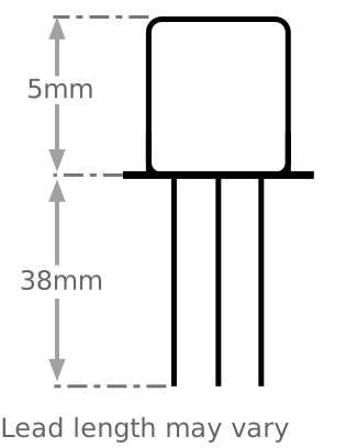
Outline:
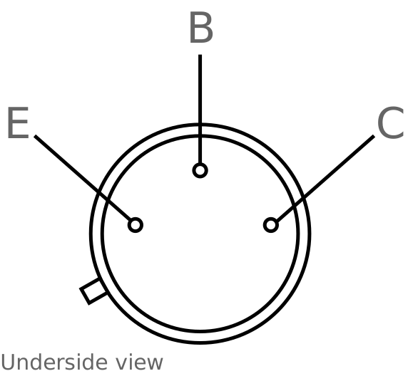
Pinout:
Explanation of transistor parameters
| Parameter | Explanation |
|---|---|
| VCBO Max | Maximum collector-base voltage with emitter open circuit . |
| VCEO Max | Maximum collector-emitter voltage with base open circuit. |
| VEBO Max | Maximum emitter-base voltage with collector open circuit. |
| VCEsat (included where applicable) | The voltage drop across the collector-emitter when the transistor is fully saturated (acting as a closed switch). |
| IC Max | Maximum collector current. |
| Parameter | Explanation |
|---|---|
| TJ | Maximum junction temperature. |
| PTOT Max | Maximum device dissipation normally in free air at 25°C unless other conditions indicated. |
| fT Min | Minimum cutoff frequency at which the current gain in a common emitter circuit falls to unity. |
| COB Max | Maximum collector capacitane, normally measured with emitter open circuit. |
| hFE | DC current gain for HFE at IC. [Note hfe is the small signal gain and although this may be slightly different, the transistor current gain will vary considerably from ne transistor to the next of the same type.] |
| PTOT Max | Maximum device dissipation normally in free air at 25°C unless other conditions indicated. |
These are the main transistor parameters that have been included in our list. There are others, but these help quantify the main elements of the performance of the transistor.
Please note, that the data given is the best estimate we can give within a tabulated summary of this nature. Parameters also vary between manufacturers. Electronics Notes cannot accept any responsibility for errors, inaccuracies, etc, although we do endevaour to ensure the data is as accurate as possible.
Video: The 2N2222: The Legendary Transistor That Won’t Die
Notes and supplementary information
The 2N2222 and 2N2222A are switching transistors which are ideal for many applications and they work well, even for some RF applications, although it's best to use a proper RF transistor for this.
As the 2N2222A is the superior version, most manufacturers tend to offer on this version these days as there is little demand for the older 2N2222 where the A version is available at the same cost.
• Availability & sources
The 2N2222A is available from a number of stockists and electronic component distributors many of which are given in the table below.
2N2222A Component Distributor, Stock and Pricing
• Notation
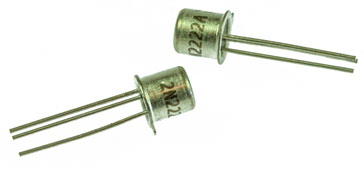
The 2N2222 and 2N2222A are normally expected to have a small metal TO18 can. A version of the 2222 transistor is available in a plastic encapsulation and this is normally designated the PN2222, but some devices in a plastic encapsulation have been seen bearing the 2N2222 designation.
• Notable features
The 2N2222 is a versatile NPN bipolar junction transistor (BJT) designed for general-purpose amplification and switching, celebrated for its reliability and widespread use in electronics since the 1960s.
High Current Gain : hFE range of typically 100 - 300, enabling efficient signal amplification with low base current.
Low Saturation Voltage : VCE(sat) as low as 0.3 V at 150 mA collector current, ideal for low-loss switching.
Fast Switching Speed : Transition frequency (fT) up to 300 MHz, supporting high-frequency applications like RF.
High Power Handling : Maximum collector current of 800 mA and power dissipation of 625 mW (TO-18 package), suitable for medium-power circuits.
Robust Voltage Ratings : VCEO breakdown voltage of 40 V, with wide operating temperature from -65°C to 175°C.
Low Noise Performance : Optimized for low-noise amplification in audio and sensor interfaces.
Compact Packaging Options : Available in TO-18 metal can or TO-92 plastic (often as a PN2222) for easy integration in through-hole designs.
Cost-Effective and Ubiquitous : Military-grade heritage (MIL-PRF-19500) ensures high reliability at low cost for hobbyist and production use.
• Typical applications summary (Figures typically refer to the 2N2222A)
| Application Category | Typical Use Case | Device Feature Utilised |
|---|---|---|
| General Switching | Relay drivers and LED control in logic circuits. | Low VCE(sat) (0.3 V) and 800 mA current rating for efficient on/off operation. |
| Audio Amplifiers | Preamp stages in microphones and small speakers. | High hFE (100-300) and low noise for clean signal amplification. |
| RF Circuits | Oscillators and modulators in amateur radio. | 300 MHz fT for high-frequency performance. |
| Sensor Interfaces | Signal conditioning for temperature/humidity sensors. | Wide temperature range (-65°C to 200°C) and robust biasing flexibility. |
| Logic Level Shifting | Interface between TTL/CMOS logic families. | 40 V VCEO and fast switching for reliable level translation. |
• 2N2222 development
The development of the 2N2222 transistor was a major milestone in the history of semiconductor device technology development.
It was developed in the early 1960s by the engineering team at Motorola. In the early 1960s, Motorola was pushing the boundaries of silicon technology to replace the less reliable and more heat-sensitive germanium devices that were normal then. Silicon technology was still relatively new.
Under the guidance of key designer John Haenichen, the team created a device that balanced high-speed switching capabilities with relatively high power handling in a compact (i.e. not a power device), manufacturable form factor.
The device was officially unveiled to the engineering world at the 1962 IRE (Institute of Radio Engineers) Convention. Its introduction marked the real beginning of the technology shift toward silicon NPN epitaxial planar techniques for bipolar transistors.
Its specific construction technique set it apart; by using planar technology, the junction areas were protected by a layer of silicon dioxide, which dramatically increased the reliability and consistency of the components during mass production.
Structurally, the 2N2222 was engineered to be robust. Its design as an epitaxial planar transistor allowed for a very thin base region, which directly contributed to its high-frequency performance and fast switching speeds.
By the standards of 1962, the device’s ability to handle collector currents up to 800mA and provide a high current gain made it remarkably versatile, enabling it to bridge the gap between low-power signal processing and medium-power driving applications.
The revolution brought by the 2N2222 lay in its groundbreaking combination of performance and cost. The 2N2222 eliminated this trade-off between performance and ruggedness, becoming the industry’s first true "jelly bean" component. Its architecture was so efficient that it could be manufactured by the millions with high yields, which eventually drove the price down to levels that made sophisticated circuit design accessible to hobbyists and commercial manufacturers alike.
Over the decades, the 2N2222 solidified its status as perhaps the most produced and recognized transistor in history. Its robust design and epitaxial planar structure proved so effective that even today, in an era of advanced MOSFETs, SiC and Gallium Nitride devices, the 2N2222 remains a relevant electronic component even today.
• Plastic Versions: PN2222A and P2N2222A
As the TO18 can is an expensive can in which to package the devices, especially as costs are driven down, the basic 2222A device is often seen in plastic packages.
Normally the devices in plastic packages should be designated with a P instead of the 2 at the beginning of the part number, but both PN2222A and 2N2222A plastic packaged devices are seen.
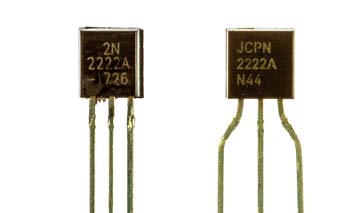
These perform well, and they use basically the same die as the TO18 packaged devices. The main performance difference is that the power handling capability is reduced.
However there is a trap waiting to catch the unwary. There is a device with the part number P2N2222A (not PN2222A but P2N2222A). This version was famously produced by OnSemiconductor and is effectively the same as the PN2222A but with the pinout inverted.
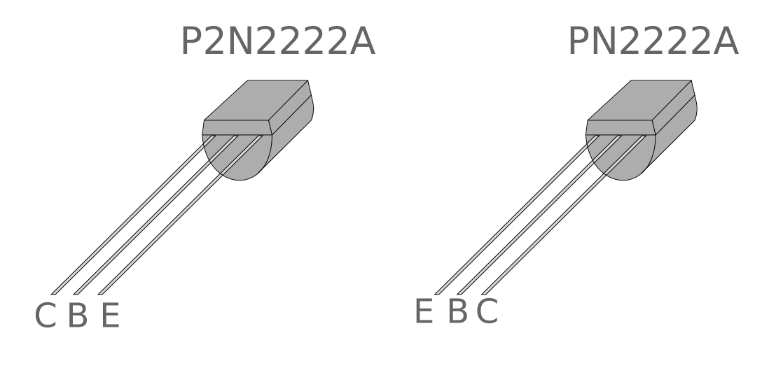
it is really important when replacing these transistors to make sure the correct pinout version is used.
 Written by Ian Poole .
Experienced electronics engineer and author.
Return to Component Data menu . . .