Home » Component data » JFET data » this page
BF245 JFET Data
Data for the BF245 JFET including electrical parameters, maximum current and voltage, pin connections, package type and many other datasheet details.
The BF245 devices are general purpose N-channel symmetrical junction JFETs intended for use as LF, HF and DC amplifiers with frequencies up to about 700 MHz.
The BF245 is a popular component among hobbyists and electronics designers due to its low noise and high gain characteristics.
These features make it an excellent choice for building radio receivers, pre-amplifiers, and other sensitive front-end circuits.
Unlike bipolar junction transistors (BJTs), JFETs are voltage-controlled devices, with the BF245 having a very high input impedance.
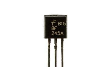
The BF245 operates in the depletion mode, meaning it is normally "on" when no voltage is applied to the gate. The BF245 comes in a standard TO-92 package, making it easy to integrate into a variety of through-hole circuit designs.
Key details and performance parameters for the BF245 JFET.
| BF245 JFET datasheet parameters & data |
|
|---|---|
| Parameters | Details |
| Brief description | N-channel symmetrical junction general purpose JFET |
| Package type | TO92 |
| Operational mode | Depletion |
| Channel type | N-channel |
| Drain to Source voltage VDS | ±30V |
| Gate to source voltage (open source) VGDO | -30V |
| Gate to source voltage (open drain) VGSO | -30V |
| Gate to source cutoff voltage VGS(off)) | -0.25V min, -8V max |
| Maximum drain current ID | 25mA |
| Drain current IDSS | 2mA min, 6.5mA max for VDS = 15V and VGS = 0V |
| Gate threshold voltage VGS(th) | |
| Forward transfer admittance ffs | 3 min, 6.5max with VDS = 15V, VGS = 0V f = 1 kHz |
| Transfer reverse capacitance Crs | 1.1pF |
| TJ °C | 150°C |
| PTOT mW | 300mW |
| Primary manufacturer | NXP and others |
Outlines & pinout:

Explanation of JFET parameters
| Parameter | Explanation |
|---|---|
| Operational mode | This details whether the FET is an enhancement or depletion mode |
| Channel type | The channel of the JFET can either be an N-type channel where electrons are the majority carriers or P-type where holes are the majority current carrier. |
| Drain to Source voltage VDSS | This is the maximum voltage that can be sustained between the drain and source |
| Gate to source voltage VGSS | This is the maximum voltage that can be sustained between the drain and the gate. |
| Maximum drain current continuous ID | This is the maximum current that can be carried byt he device. Sometimes there may be a differentiation between the continuous and pulsed or peak values |
| Parameter | Explanation |
|---|---|
| Zero gate voltage drain current IDSS | This is the current carried by the device when the gate voltage is zero. The test conditions are normally stated for this. |
| Gate threshold voltage VGS(th) | This is the minimum gate-to-source voltage, VGS required to create a conductive channel between the source and drain terminals |
| Static drain source ON resistance RDS(ON) | This is the resistance of the device when turned on. The test conditions of voltage and current are normally given for this. |
| Drain source ON voltage VDS(ON) | This is the voltage across the device when it is turned on. Again the test conditions are given. |
| Forward transconductance gFS | Forward transconductance also given the letters gm is defined as the change in drain current (ΔID) for a small change in the gate-source voltage ΔVGS, with the drain-source voltage, VDS held constant. |
These are the main JFET parameters that have been included in our list. There are others, but these are the main ones and they help quantify the main elements of the performance.
Please note, that the data given is the best estimate we can give within a tabulated summary of this nature. Parameters also vary between manufacturers. Electronics Notes cannot accept any responsibility for errors, inaccuracies, etc, although we do endevaour to ensure the data is as accurate as possible.
Notes and supplementary information
• Availability & sources
The BF245 is available from a number of stockists and electronic component distributors many of which are given in the table below.
BF245 Component Distributor, Stock and Pricing
• Further details
The BF245 devices are general purpose N-channel symmetrical junction JFETs, i.e. the drain and source are interchangeable, and they are intended for use as LF, HF and DC amplifiers with frequencies up to about 700 MHz.
 Written by Ian Poole .
Experienced electronics engineer and author.
Return to Component Data menu . . .