Logic Supply Decoupling Techniques
- notes on the techniques for effective supply line decoupling for logic / digital integrated circuit boards.
Logic / Digital Design Guidelines Includes:
Design guidelines overview
Supply decoupling
PCB groundplane usage
Unused gates
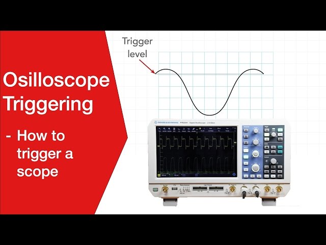
It is important to ensure that the supply line to any circuit is properly decoupled to ensure that noise and other signals are not transferred from one area of the circuit to another.
While logic circuits are based around digital signals, there is a still a real need for circuits to be properly decoupled.
It is common for switching spike to appear on the power supply lines and if there are significantly large, they can falsely trigger counters, flip-flops, registers and the like.
as a result, it is very important to ensure that supply line decoupling is implemented across any digital circuit board.
Typical supply line noise
Although each circuit and circuit board will be different, there are common factors that affect all digital circuit boards.
The ripple and noise on the supply lines has some common traits dependent upon the circuit conditions.
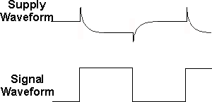
The waveforms shown below are of the signal and the expected impact it has on the supply line. The spikes are caused by the very high speed output drivers in the digital circuits. Spikes of current are required to drive charge the capacitance in the signal lines. As the lines charge up and come up to the required voltage, the current required falls and the supply line returns to its nominal voltage.
If left unchecked these spikes could be sufficient in magnitude to cause corruption to some of the circuits on the board.

Switching spikes appearing on a digital / logic supply line
Dependent upon the circuit layout, the spikes may even undergo some ringing rather than fading way exponentially as shown.
If an appreciable amount of current is being drawn from the output of a logic chip, it may apply further ripple onto the supply line beyond the spikes. The line voltage may fall slightly, thereby modulating the supply line even more.
Digital / logic supply line switching spikes and voltage variation
as a result of higher current drawn from logic output device
It can be seen that when the signal output is high more current could be drawn and this could result, as shown in the supply voltage level falling.
This noise can then be transferred around the board if not reduced to an acceptable level giving rise to problems anywhere within the circuit.
In addition to this form of noise, general noise from the power supply and other sources may also appear. To ensure that all ICs are protected, adequate supply line decoupling should be incorporated.
Applying decoupling to logic supply line
With the very high speeds of switching that occur in current logic circuits, it is necessary to ensure that the decoupling is applied in the most effective way. Even small amounts of inductance from PCB lines or other effects can have a significant effect and render the decoupling considerably less effective.
In addition to this, the low voltages and tight limits on the supply requirements mean that it is not possible to use CR filtering to reduce the level of spikes and ripple.
In order to overcome the effects of the stray inductance inherent in any PCB track or other wire, it is normal practice to distribute the decoupling across the board.
Typically this is achieved by providing a form of bulk decoupling (normally a small decoupler for high frequency noise and a larger one to remove low frequency variations) at the entry point for the supply to the board, or at the output of an on-board regulator if this is applicable. In addition to this local decoupling is then provided for each logic chip.

Typical digital / logic supply line decoupling arrangement
The capacitors for low frequency and high frequency decoupling have very different values. The "bulk" capacitance normally consists of a small tantalum capacitor - tantalum has a better high frequency performance with lower inductance than an electrolytic and they are mow widely used on surface mount boards because the technology can be contained within the SMD packages that are normally used. A value of around 22 µF is often satisfactory. If there is a large number of devices on the board then it may be necessary or wise to add a couple around the board, especially so that longer power line runs on the board are adequately decoupled.
The smaller capacitors for individual integrated circuits are placed as close as possible to the power connections. Sometimes they are placed on the reverse side of the board, under the IC itself to ensure that the connections are as short as possible. With the frequencies often used today, even lengths of a centimetre can add inductance. The values may vary between 10 and 100 nF, but some experimentation may be needed dependent upon the technology, layout, etc. This capacitance will be needed to supply the peak current required by the integrated circuit during switching.
The value of the capacitor will depend upon the chips and technology in use
Typical decoupling capacitor guidelines may be:
- One bulk capacitor of around 22µF per board preferably tantalum.
- One 1µF capacitor per 10 - 20 SSI / MSI devices or 2 - 5 LSI devices.
- One 10 - 100 nF capacitor per supply pin of each IC with leads as short as possible across the supply and ground pins.
 Written by Ian Poole .
Experienced electronics engineer and author.
More Digital Logic and Embedded Topics:
FPGA programming
Embedded systems
How a computer works
Logic circuit design basics
Logic / circuit design guidelines
Return to Digital / Logic / Processing menu . . .