Invention of the FET: Field Effect Transistor
The invention of the field effect transistor, FET was another major step forward in semiconductor history enabling advances in many areas including integrated circuits.
Transistor History Includes:
Transistor history
First silicon transistor
Phototransistor invention
FET invention
More semiconductor history
History of semiconductor technology development
PN junction diode invention
Invention of the integrated circuit
The invention of the field effect transistor, FET, proved to be elusive for many years with a number of people postulating ideas but not being able to make a real device.
The history of the field effect transistor is interesting because the first ideas for the invention of the field effect transistor appeared surfaced in the 1920s, and when Bardeen, Brattain and Schockley invented the point contact transistor they had been intending to make a FET, but could not get it to work.
Accordingly the invention of the field effect transistor was a major hurdle and it took improvements in semiconductor refining as well as fabrication technologies and in particular the development of oxide layers on silicon to enable this electronic component to be made properly.
However once the field effect transistor had been invented it became a major enabler for integrated circuits as the lower current levels and hence lower heat dissipation offered by FET technology enabled integration levels to dramatically increase. Without the use of low power FET technology the heat levels would limit the number of devices on a chip. Accordingly these electronic components would not be what they are today without the invention of the field effect transistor and in particular the MOSFET.
What is a FET?
The technology behind the FET enables the field effect transistor to provide high levels of performance. Using an electric field to control the current in a piece of semiconductor, it has a very high input impedance when compared to the bipolar transistor.
The fact that the FET uses an electric field as the control mechanism means it is a voltage device like a vacuum tube / valve and not a current driven device like a bipolar transistor. There are significant differences between these two electronic components.
Note on Field Effect Transistor Technology:
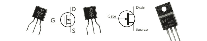
The field effect transistor, FET, is a three terminal device which provides voltage gain. Having a high input impedance the electric field in the vicinity of the input terminal called the gate modifies the current flowing in what is called the channel between terminals called the source and drain.
Read more about the Field Effect Transistor Device & How it Works
First field effect ideas
The first ideas for a field effect device started to appear quite early on in the overall history of the transistor and semiconductors in general.
The first idea for a field effect device was patented by an Austro-Hungarian physicist named Julius Edgar Lilienfeld in 1925.
Lilienfeld had started working on the physics behind electrons and particles in a vacuum in 1905 and he identified field electron emission. For this work he was based in the Physics Department of the University of Leipzig.
He continued to work on electrical particles and electron physics looking into the field effects associated with them.
As a result of this work he conceptualised a field effect device and applied for his patent on 8 October 1926 as a “method and apparatus for controlling electric currents.” This patent was then granted on 28 January 1930. Lilienfeld had actually filed two other patents in 1928, but the one granted in January 1930 appears to be the most important.
Lilienfeld went on to make other contributions to electrical and electronic science developing the electrolytic capacitor and investigating X-rays.
By the time Lilienfeld had applied for his field effect patent, he had moved to the US in 1921 in order to pursue his patent claims and he resigned his professorship to stay in the USA permanently in 1926. He finally became a US citizen in 1934.
Although Lilienfeld had described the concept for a field effect device, he was unable to make one to demonstrate the principle and although he made some major advances in thinking, Lilienfeld did not actually invent the field effect transistor as a realisable electronic component.
More moves toward FET invention
Like many developments, the invention of the field effect transistor involved a number of people thinking along the same lines around the same time.
Another researcher named Oskar Heil, was a German physicist who spent some of his career working at the cavendish Laboratory at the University of Cambridge was well as some time at the British company, Standard Telephones and Cables, STC. However he returned to Germany before the onset of war.
Nevertheless, Oscar Heil described the possibility of controlling the resistance in a semiconducting material by the use of an electric field in a British patent in 1935.
This was another step forwards towards the invention of the realisable field effect transistor.
New focus on FET invention at Bell Labs
During the Second World War, there had been a major drive to push forward new electronics technology that could improve electronics in many ways. Bell labs had been one of the main areas where this work was being carried out, although a number of almost parallel lines of research were being funded by the US government to ensure that nothing was missed and developments were moved on as quickly as possible.
One team working at Bell Labs was particularly key to the actual developments made.
John Bardeen and Walter Houser Brattain while working under William Shockley at Bell Labs in 1947 observed the field effects shortly after the 17-year expiry on the field effect device patents expired.
Initially the team had tried to make a working field effect transistor by modulating the conductivity of a section of semiconductor using an external field.
They were unsuccessful in doing this mainly because of problems with the surface states in the semiconductor sample, the dangling bond, and the germanium and copper compound materials. The field effect transistor invention needed to wait until these problems could be solved.
All was not lost because the work was repurposed and the first point contact transistor was invented in 1947.
This was followed shortly afterwards by Shockley building on the first transistor technology and developing the first bipolar junction transistor in 1948.
First successful FET device
The first successful invention of a field effect transistor appears to be a junction field effect transistor that was patented by Heinrich Welker in 1945.
There also appears to be another associated invention of a form of junction field effect transistor called a static induction transistor by Japanese engineers Jun-ichi Nishizawa and Y. Watanabe in 1950.
Shockley continued to work on the concept of a device that used the field effect as the basis of its operation. He investigated the concept further and produced a paper in 1952. Building on this George F. Dacey and Ian M. Ross made a working junction field effect transistor in 1953. Even though this was a considerable achievement, these electronic components were both large and difficult to make.
Metal oxide silicon, MOS developed
Even though the junction field effect transistor had been invented, it was not the end of the story as the performance was not as good as it had been hoped other forms of the device might be.
When investigating their field effect device in 1947, Bardeen, Brattain and Shockley explained the failure of their device in terms of the surface states that existed on the semiconductor and these were trapping electrons and this blocked or shield the channel or conducting area of the semiconductor from the external field.
To overcome this, Shockley patented the idea of using an inversion layer instead of the very thin layer of the semiconductor material. The concept was that this layer would confine the flow of minority carriers and this would increase the level of modulation or control and hence the control the conductivity better.
In 1948, using this theory as the basis for further work Bardeen patented the concept of an insulated gate FET that used an inversion layer.
The main breakthrough for the MOSFET invention came about as a result of an Egyptian engineer named Mohamed Atalla. In the late 1950s he demonstrated some experimental work showing tat growing a thin layer of silicon oxide on a clean silicon surface neutralised the surface states which had caused the barrier to the operation of a field effect transistor before.
This work was then developed even further so that in 1959 the first metal-oxide-silicon field effect transistor, MOSFET was invented by Mohamed Atalla and Dawon Kahng.
Further developments took place elsewhere. A year later in 1960 Karl Zaininger and Charles Meuller at RCA fabricated an MOS transistor and also C T Sah of Fairchild built a tetrode MOS device. Further developments took place integrating MOSFET technology containing a number of devices onto a single chip in 1962 with an experimental 16-transistor integrated device at RCA. This work was carried out by Fred Heiman and Steven Hofstein.
The invention of the field effect transistor had a major impact on electronics technology. In particular the MOSFET, in its format as CMOS (Complementary MOS) and its low level of current consumption allowed the levels of integration to increase very significantly. It had been postulated that the limit on IC integration would not be that high because of the level of heat generated. Changing to CMOS technology allowed dissipation to be reduced by many factors and integration levels to rise similarly. This opened the door to large scale integration, microprocessors and all the other digital technology we take for granted today.
Field effect transistor technology is used in many electronic components from the discrete and surface mount devices, SMDs to microprocessors, FPGAs, semiconductor memory devices and a whole lot more. Without FET technology, many of today's electronic components would not exist.
 Written by Ian Poole .
Experienced electronics engineer and author.
More History:
Radio history timeline
History of the radio
Ham radio history
Coherer
Crystal radio
Magnetic detector
Spark transmitter
Morse telegraph
Valve / tube history
PN junction diode invention
Transistor
Integrated circuit
Quartz crystals
Classic radios
Mobile telecoms history
Vintage mobile phones
Return to History menu . . .