What is a FET: Field Effect Transistor: Types, Technology, . .
The Field Effect Transistor, FET, is a three terminal active device that uses an electric field to control the current flow and it has a high input impedance which is useful in many circuits.
Home » Electronic components » this page
FETs, Field Effect Transistors Includes:
FET basics
FET specifications
JFET
MOSFET
Dual gate MOSFET
Power MOSFET
MESFET / GaAs FET
HEMT & PHEMT
FinFET technology
IGBT
IGBT vs MOSFET - which is better?
Silicon carbide, SiC JFET
Silicon carbide, SiC MOSFET
Silicon carbide vs silicon MOSFETs
GaN FET / HEMT
SiC vs GaN
FET component data:
MOSFETs
SiC MOSFETs
GaN FETs
IGBTs
The field effect transistor, FET is a key electronic component using within many areas of the electronics industry.
The FET used in many circuits constructed from discrete electronic components in areas from RF technology to power control and electronic switching to general amplification.
However the major use for the field effect transistor, FET is within integrated circuits. In this application FET circuits consume much lower levels of power than ICs using bipolar transistor technology. This enables the very large scale integrated circuits to operate. If bipolar technology was used the power consumption would be orders of magnitude greater and the power generated far too large to dissipate from the integrated circuit.
Apart from being used in integrated circuits, discrete versions of these semiconductor devices are available both as leaded electronic components and also as surface mount devices.
Field Effect Transistor, FET history
Before the first FETs were introduced into the electronic components market, the concept of these semiconductor devices had been known for a number of years. There had been many difficulties in realising this type of device and making it work.
Some of the early concepts for the field effect transistor were outlined in a paper by Lilienfield in 1926, and in another paper by Heil in 1935.
The next foundations were set in place during the 1940s at Bell Laboratories where the semiconductor research group was set up. This group investigated a number of areas pertaining to semiconductors and semiconductor technology, one of which was a device that would modulate the current flowing in a semiconductor channel buy placing an electric field close to it.
During these early experiments, the researchers were unable to make the idea work, turning their ideas to another idea and ultimately inventing another form of semiconductor electronics component: the bipolar transistor.
After this much of the semiconductor research was focussed on improving the bipolar transistor, and the idea for a field effect transistor was not fully investigated for some while. Now FETs are very widely used, providing the main active element in many integrated circuits. Without these electronic components electronics technology would be very different to what it is now.
Note on Field Effect Transistor Invention & History:
The field effect transistor took many years to develop. The first ideas for the concept appeared in 1928, but it was not until the 1960s that they started to become widely available.
Read more about the Field Effect Transistor Invention & History
Field Effect Transistor – the basics
The concept of the field effect transistor is based around the concept that charge on a nearby object can attract charges within a semiconductor channel. It essentially operates using an electric field effect - hence the name.
The FET consists of a semiconductor channel with electrodes at either end referred to as the drain and the source.
A control electrode called the gate is placed in very close proximity to the channel so that its electric charge is able to affect the channel.
In this way, the gate of the FET controls the flow of carriers (electrons or holes) flowing from the source to drain. It does this by controlling the size and shape of the conductive channel.
The semiconductor channel where the current flow occurs may be either P-type or N-type. This gives rise to two types or categories of FET known as P-Channel and N-Channel FETs.
In addition to this, there are two further categories. Increasing the voltage on the gate can either deplete or enhance the number of charge carriers available in the channel. As a result there are enhancement mode FET and depletion mode FETs.

As it is only the electric field that controls the current flowing in the channel, the device is said to be voltage operated and it has a high input impedance, usually many megohms. This can be a distinct advantage over the bipolar transistor that is current operated and has a much lower input impedance.

FET circuits
Field effect transistors are widely used in all forms of electronic circuit designs from those used in circuits with discrete electronic components, to those employed in integrated circuits.
Note on Field Effect Transistor Circuit Design:
The field transistor transistors can be used in many types of circuits although the three basic configurations are common source, common drain (source follower) and common gate. The circuit design itself if fairly straightforward and can be undertaken quite easily.
Read more about Field Effect Transistor Circuit Design
As the field effect transistor is a voltage operated semiconductor device rather than a current device like the bipolar transistor, this means that some aspects of the circuit are very different: the bias arrangements in particular. However electronic circuit design with FETs is relatively easy - it is just a bit different to that using bipolar transistors.
Using FETs, circuits like voltage amplifiers, buffers or current followers, oscillators, filters and many more can all be designed, and the circuit designs are very similar to those for bipolar transistors and even thermionic valves / vacuum tubes, although the bias arrangements are different. Interestingly valves / tubes are also voltage operated devices, and therefore their circuit designs are very similar, even in terms of the bias arrangements.
Field Effect Transistor types
There are many ways to define the different types of FET that are available. The different types mean that during the electronic circuit design, there is a choice of the right electronic component for the circuit. By selecting the right device it is possible to obtain the best performance for the given circuit.
FETs may be categorised in a number of ways, but some of the major types of FET can be covered in the tree diagram below.

Click on image for larger version
There are many different types of FET on the market for which there are various names. Some of the major categories are delayed below.
Junction FET, JFET: The junction FET, or JFET uses a reverse biased diode junction to provide the gate connection. The structure consists of a semiconductor channel which can be either N-type or P-type. A semiconductor diode is then fabricated onto the channel in such a way that the voltage on the diode affects the FET channel.
In operation this is reverse biased and this means that it is effectively isolated from the channel - only the diode reverse current can flow between the two. The JFET is the most basic type of FET, and the one that was first developed. However it still provides excellent service in many areas of electronics.
Read more about . . . . junction field effect transistor, JFET.
Insulated Gate FET / Metal Oxide Silicon FET MOSFET: The MOSFET uses an insulated layer between the gate and the channel. Typically this is formed from a layer of oxide of the semiconductor.
The name IGFET refers to any type of FET that has an insulated gate. The most common form of IGFET is the silicon MOSFET - Metal Oxide Silicon FET. Here, the gate is made of a layer of metal set down on the silicon oxide which in turn is on the silicon channel. MOSFETs are widely used in many areas of electronics and particularly within integrated circuits.
The key factor of the IGFET / MOSFET is the exceedingly gate high impedance these FETs are able to provide. That said, there will be an associated capacitance and this will reduce the input impedance as the frequency rises.
Read more about . . . . Metal Oxide Silicon FET, MOSFET.
Dual Gate MOSFET: This is a specialised form of MOSFET that has two gates in series along the channel. This enables some considerable performance improvements to be made, especially at RF, when compared to single gate devices.
The second gate of the MOSFET provides additional isolation between the input and output, and in addition to this it can be used in applications like mixing / multiplication.
Read more about . . . . Dual Gate MOSFET.
MESFET: The MEtal Silicon FET is normally fabricated using Gallium Arsenide and is often referred to as a GaAs FET. Often GaAsFETs are used for RF applications where they can provide high gain low noise performance. One of the drawbacks of GaAsFET technology results from the very small gate structure, and this makes its very sensitive to damage from static, ESD. Great care must be taken when handling these devices.
Read more about . . . . MESFET / GaAsFET.
HEMT / PHEMT: The High Electron Mobility Transistor and Pseudomorphic High Electron Mobility Transistor are developments of the basic FET concept, but developed to enable very high frequency operation. Although expensive, they enable very high frequencies and high levels of performance to be achieved.
Read more about . . . . HEMT / PHEMT.
FinFET: FinFET technology is now being used within integrated circuits to enable higher levels of integration to be achieved by allowing smaller feature sizes. As higher density levels are needed and it becomes increasingly difficult to realise ever smaller feature sizes, FinFET technology is being used more widely.
Read more about . . . . FinFET.
VMOS: VMOS standard for vertical MOS. It is a type of FET that uses a vertical current flow to improve the switching and current carrying performance. VMOS FETs are widely used for power applications.
Although there are some other types of field effect transistor that may be seen in the literature, often these types are trade names for a particular technology and they are variants of some of the FET types listed above.
FET specifications
Apart from selecting a particular type of field effect transistor for any given circuit design, it is also necessary to understand the different specifications. In this way it is possible to ensure that the FET will operate to the required performance parameters.
FET specifications include everything from the maximum voltages and currents permissible to the capacitance levels and the transconductance. These all play a part in determining whether any particular FET is suitable for a given circuit or application.
Field affect transistor technology can be used in a number of areas where bipolar transistors are not as suitable: each of these semiconductor devices has its own advantages and disadvantages, and can be used to great effect in many circuits. The field effect transistor has a very high input impedance and is a voltage driven device and this opens it up to being used in many areas.
 Written by Ian Poole .
Experienced electronics engineer and author.
More Electronic Components:
Batteries
Capacitors
Connectors
ADC
DAC
Diodes
FET
Inductors
Memory types
Phototransistor
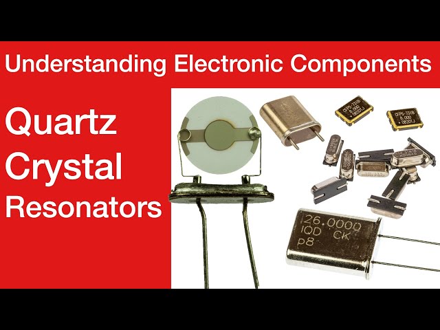
Quartz crystals
Relays
Resistors
RF connectors
Switches
Surface mount technology
Thyristor
Transformers
Transistor
Unijunction
Valves / Tubes
Return to Components menu . . .