Gallium Nitride GaN FETs & HEMTs: what they are & how they work
Gallium nitride is a semiconductor material that is being used increasingly to provide improved performance especially in high speed and RF FETs and HEMTs.
Home » Electronic components » this page
FETs, Field Effect Transistors Includes:
FET basics
FET specifications
JFET
MOSFET
Dual gate MOSFET
Power MOSFET
MESFET / GaAs FET
HEMT & PHEMT
FinFET technology
IGBT
IGBT vs MOSFET - which is better?
Silicon carbide, SiC JFET
Silicon carbide, SiC MOSFET
Silicon carbide vs silicon MOSFETs
GaN FET / HEMT
SiC vs GaN
FET component data:
MOSFETs
SiC MOSFETs
GaN FETs
IGBTs
Gallium nitride, GaN FETs or GaN transistors are being used increasingly in many power modules and devices as well as for RF power circuit designs. Often the terms GaN HEMT and GaN transistor are used interchangeably.
The very high electron mobility of gallium nitride, GaN enables the fabrication of semiconductor devices that have a low value of ON resistance combined with a very high switching frequency capability.
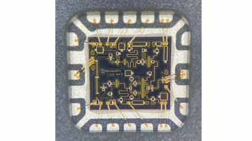
Photo courtesy of PRFI Ltd
These benefits mean that GaN FETs are being used in many new electronic circuit designs for everything from power systems, for electric vehicles and renewable energy applications to RF power amplifiers, other RF design circuits and the like.
GaN FETs use the interface between two semiconductor materials to produce a very thin region known as the 2DEG (see below for an explanation) to provide very high levels of electron mobility that result in GaN HEMTs or high electron mobility transistor being formed.
Often GaN transistor technology is used to fabricate monolithic microwave ICs, MMICs which provide high levels of performance at microwave frequencies.
What is gallium nitride
Gallium nitride is a compound semiconductor material using materials from groups III & V in the periodic table of elements.
Physically the material is very hard, and has a Knoop hardness factor of 14.21 GPa and GaN has some other interesting physical attributes, but it is the electrical properties that are of interest here.
Gallium nitride has a wide bandgap of 3.5eV which is very similar to that of silicon carbide and this makes it very suitable as a semiconductor for a number of devices.
GaN has some very useful properties that make it ideal for a number of power applications. It can tolerate a high operating voltage, handle high levels of power, and it can operate at high frequencies making it ideal for many RF applications from mobile communications, 5G, 6G, etc to aerospace, and satellite communications.
Note on Gallium Nitride:
Gallium nitride is a semiconductor material that is physically very hard, but also acts as a semiconductor that has a wide bandgap, and enables high power levels to be used at high frequencies when used in semiconductor devices.
Read more about Gallium Nitride, GaN.
For manufacture of the GaN electronics components themselves, gallium nitride needs to be formed on what is often termed a pseudo-substrate - it is not possible to make a substrate of GaN itself for chemical reasons.
Typically GaN is deposited on either silicon or silicon carbide to give GaN on Silicon, ofter referred to as Gan on Si or GaN on Silicon carbide referred to as GaN on SiC.
GaN on silicon devices are cheaper than those of GaN on silicon carbide, but the GaN on SiC offers a number of advantages:
GaN on SiC has higher thermal conductivity: Owing to the higher thermal conductivity of silicon carbide, the overall GaN on SiC has a higher thermal conductivity, typically three times that of the GaN on silicon. This means that GaN on SiC devices have a higher efficiency, higher reliability and higher power density when compared to GaN on silicon devices of the same geometry.
Silicon carbide has lower relative permittivity: The low relative permittivity of silicon carbide means that GaN on SiC devices can have a higher bandwidth than GaN on silicon devices.
Another possibility for a substrate is synthetic diamond. This offers a high level of thermal conductivity, but the cost is much higher than that of both GaN on silicon and GaN on SiC.
What is 2DEG
There are many websites and informational articles about HEMTs that refer to 2DEG without an explanation of what it is.
In essence 2DEG stands for 2-dimensional electron gas and it is a core concept behind HEMT technology.
The basic concept behind this is explained below.
GaN HEMT concept
GaN FETs or GaN transistors are essentially high electron mobility transistors or HEMTs. The concept of the HEMT has been known for many years and has been employed in other FET technologies.
The chemical structure of the gallium nitride is referred to as a "Wurtzite" structure. It is this structure that is the key to the HEMT operation of the GaN transistors.
The Wurtzite structure of the GaN crystal give the material a piezoelectric effect. This is predominantly achieved because of charged elements within the crystal lattice. If the structure is subjected to strain, then the deformation will cause a very small shift in the atoms in the lattice that generate an electric field: the higher the level of strain, the greater the electric field is that is created.
When the aluminium gallium nitride, AlGaN layer is grown on top of the gallium nitride, GaN crystal, the interface between the two crystal lattices does not completely match and therefore a strain is set up.
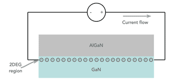
The strain induces a 2 dimensional electron gas, 2DEG. This two dimensional electron gas is highly conductive because the electrons are confined within a very small region at the interface. This virtually doubles the electron mobility from about 1000 cm2/V ˙ s in normal GaN to between 1500 and 2000 cm2/V ˙ s within the 2DEG region. This high electron concentration and mobility is the basis for HEMTs and in this case the GaN HEMT.
It is found that the quality of 2DEG has a significant impact on the electronic transport along the interface and hence to properties of final devices.
The flow of electrons through the two dimensional region - effectively the channel - is controlled by the gate potential in the normal way for a FET.
GaN transistor structure & operation
All GaN FETs or HEMTs employ the same basic technology and utilise the HEMT structure with its two dimensional electron gas region providing the fundamental mode of operation for the device.
GaN HEMTs are available in both depletion mode and enhancement mode varieties.
Depletion mode: A depletion mode GaN transistor is normally on; and to turn it off, a negative voltage relative to the drain and source electrodes must be applied to the gate.
Enhancement mode: Enhancement mode or e-mode FETs are those that are normally off. They are turned on by applying a positive voltage to the gate relative to the drain and source.
Naturally the structures of the actual FETs are slightly different for both types. Also there are a number of approaches that are adopted by different manufacturers of these electronic components, but the basic principles of operation are exactly the same.
Depletion mode GaN transistor
The basic structure for a depletion mode GaN HEMT consists of the three electrodes, source, drain and gate as would normally be expected for a field effect transistor.
The source and drain are fabricated so they do not sit on the AlGaN layer, but instead they contact directly with the GaN region and hence the 2DEG.

As this is a depletion mode HEMT, this creates a short circuit between the drain and the source.
To reduce the flow of electrons through the 2DEG a negative potential is applied to the gate relative to the drain and source, this depletes the channel of electrons, thereby reducing the channel conductivity.
There are a number of ways in which these devices can be fabricated. It is possible to create a Schottky gate electrode by depositing a metal layer directly on top of the AlGaN using details like Nickel-gold or platinum. A Schottky barrier was created that enabled the channel conductivity to be controlled.
Deletion mode GaN HEMTs have also been fabricated using an insulating layer and then depositing a metal gate onto this. This approach bears many similarities with silicon MOSFET technology.
Whilst depletion mode transistors are applicable in many electronic circuit designs, they tend not to be used for power systems because it is not advisable to have the large current source often available in power systems, with a device that is short circuit when turned on.
Enhancement mode GaN transistor
There are several methods that have been used to create enhancement mode GaN transistors. Typically they are a little more involved to fabricate, but they tend to be mode widely used.
There are five main structures that are used for enhancement mode GaN FETs. These are: cascode hybrid, direct drive hybrid, implanted gate, pGaN gate, and the recessed gate.
Some of the main structure techniques are described below:
Implanted gate: One method for creating an enhancement mode GaN FET is to implant fluorine atoms into the AlGaN barrier layer in the region of the gate. The fluorine atoms create a negative charge in the AlGaN layer and this depletes the electrons from the 2DEG plane in this region.

Basic structure concept for a implanted gate enhanced mode GaN HEMT The Schottky gate on top of this region provides control because when a positive bias is applied, electrons will be attracted back into the 2DEG plane in this region and current will flow. in the channel.
Recessed gate structure: The recessed gate structure is created by thinning the AlGaN barrier region above the 2DEG plane. This reduces the voltage generated by the piezo-electric effect in this region. A point is reached where the voltage generated by the stress in the crystal structure is less than the built in voltage of the Schottky metal gate and with zero bias the 2DEG plane is eliminated here.

Basic structure concept for a recessed gate enhanced mode GaN HEMT If a positive bias is placed on the gate, electrons are attracted back to the interface between the two semiconductor material and current is able to flow dependent upon the level of bias.
With GaN semiconductor technology developing at a rapid rate because of the advantages it brings to RF design and the design of a host of power designs, there will be more developments in the coming years and new formats and structures for devices.
GaN transistor applications
GaN HEMT or transistor technology is used in many areas of electronics circuit design and RF design. The parameters of the GaN transistors that are produced mean that they are applicable for many different applications where high power, high frequency or high performance or any combination of these parameters are required.
Power systems: With everything from switch mode power supplies, power switching, electric vehicles and the like needing power switching devices, the GaN HEMT lends itself to many of these applications. The fast switching and low ON resistance of these devices means that efficiency levels are high. The high breakdown voltages also mean that relatively high level switching can be accomplished.
RF power amplifiers: The combination of high power capability and high speed means that GaN FET technology is an ideal candidate for RF power amplifiers.
GaN FET technology offers many advantages from high reliability, and high efficiency levels to the capability to operate at high frequencies. As a result GaN technology is used in many RF power amplifiers for a whole variety of applications including mobile communications where it is used, particularly in base stations for 5G, 6G, etc. It is also used in satellite applications where its high reliability and resilience as well as the high levels of efficiency that can be returned are of great interest.
GaN RF switches: Another application for GaN FETs is as RF switches. There are many situations where RF switching is required, and these electronic components provide the ideal means of switching the RF circuitry. They are able to handle much higher power levels than the GaAsFETs that are also used in RF designs for switching.
GaN FETs are able to use the same basic RF design architecture as GaAsFET switches, but with changes to the electronic comment values, etc. As RF switches, these GaN transistors are able to provide a low switching loss because of their low ON resistance, they have a high level of isolation, excellent linearity and they can handle much higher power levels than GaAsFETs.
GaN low noise amplifiers: The high frequency capability of GaN FETs means that they are able to not only operate as a power amplifier, but also on the receiving side as a front end low noise amplifier, LNA. In this role, these electronic components are able to perform well, offering a low noise figure, an essential in this role within an RF circuit design.
However, in view of their high power capability and general robustness, they are able to tolerate high input power levels, unlike GaAsFETs which can be rather susceptible to overload and ESD. Accordingly GaN FETs are starting to be used in radar installations as one of many examples.
One advantage of their high tolerance of RF levels is that a circulator may not always be needed. As the circulator will introduce loss, this can reduce the overall receiver sensitivity as well as absorbing some transmitter power.
GaN mixers: Gallium nitride FETs are also finding use within high performance RF mixers. Here, the high level of linearity these electronic components can provide and their resilience to high power levels, means that they are replacing GaAsFET based mixers in many new RF designs.
MMIC: GaN FET technology is also used within many monolithic microwave ICs, MMICs. With MMICs needing to extend their frequency ranges in a variety of RF design blocks, GaN technology is ideal for use within MMICs that provide a variety of RF functions.
There are many areas in which GaN technology is being used and as the technology develops further, there is always the possibility electronic components using GaN technology will be used in other areas.
Gallium nitride technology is becoming increasingly prevalent in many areas of power and radio frequency circuit design. The devices still cost more than soem of their equivalents using older technology, but the benefits can sometimes outweigh the cost penalties, and in many instances result in a lower overall cost of the item. Accordingly GaN FETs or GaN HEMTs are being seen in many RF designs as well as within many new circuit designs for power systems.
 Written by Ian Poole .
Experienced electronics engineer and author.
More Electronic Components:
Batteries
Capacitors
Connectors
ADC
DAC
Diodes
FET
Inductors
Memory types
Phototransistor
Quartz crystals
Relays
Resistors
RF connectors
Switches
Surface mount technology
Thyristor
Transformers
Transistor
Unijunction
Valves / Tubes
Return to Components menu . . .