What is a Transistor: How Does It Work - NPN & PNP
Description about what a transistor is, how a bipolar transistor works, and details of NPN and PNP transistors.
Home » Electronic components » this page
Transistor Tutorial Includes:
Transistor basics
Gain: Hfe, hfe & Beta
Transistor specifications
BJT Early Effect
BJT vs MOSFET - which to use
Transistor and diode numbering codes
Choosing replacement transistors
Transistor component data:
Transistor component data
Transistors are at the very core of today's electronics technology. The development of the bipolar transistor or bipolar junction transistor, BJT, has resulted in many changes to the world.
The introduction of the bipolar transistor has enabled many technologies we take for granted today: everything from portable transistor radios, through to mobile phones, and computers, remote operation, the functionality we take for granted in current day automobiles, etc . . . . All these and many more everyday items have all been made possible by the invention of the transistor.
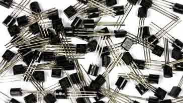
Today, bipolar transistors are available in many forms. There is the basic transistor in a leaded form or its available as a surface mount transistor. But transistors are also widely used within integrated circuits. Most digital ICs use field effect technology, but many analogue ICs use bipolar technology to provide the required performance.
Together with their field effect transistor, FET, relatives which use a very different principle, the bipolar transistor forms the basis of most of todays electronic equipment, either as discrete devices or within integrated circuits.
Transistor development
Semiconductor technology is now well established but it has been used for over a hundred years. The first semiconductor effects were noticed back in the early 1900s when the first wireless or radio sets were being used. Various ideas were being investigated as detectors.
Thermionic valve or vacuum tube technology was introduced in 1904, but these devices were expensive, and also required powering by a battery. Soon afterwards the Cat's Whisker detector was discovered. This consisted of a thin wire placed onto one of a number of types of material. These materials are known today as semiconductors and form the basis of modern electronics technology.
Note on Transistor History:
The bipolar transistor was invented by three researchers working at Bell Labroratories: John Bardeen, Walter Brattain, and William Schockley. They had been working on an idea that used a field effect to control the current in a semiconductor, but they were unable to make the idea work. They turned their focus onto another possibility and made a three terminal device using two closely spaced point contacts on a wafer of germanium. This idea worked and they were able to demonstrate it provided gain in late 1949.
Read more about Bipolar Transistor History
After the basic idea was developed, it took some time before semiconductor technology was adopted, but once it was, it took off in a major way as we know today.
What is a bipolar transistor
it is worth defining in a few words what a bipolar transistor is:
Bipolar transistor definition:
A bipolar transistor is a semiconductor device consisting of three areas either P-type or N-type - an area of one type is sandwiched between areas of the other. The transistor fundamentally amplifies current but it can be connected in circuits designed to amplify voltage or power.
A bipolar transistor needs to be differentiated from a field effect transistor. A bipolar junction transistor, BJT, gains its name from the fact that it uses both holes and electrons in its operation. Field effect transistors are unipolar devices using one or either type of charge carrier.
A bipolar transistor, or more exactly a bipolar junction transistor, BJT, has two PN diode junctions which are back to back. The bipolar transistor has three terminals, named the emitter, base and collector.
The transistor amplifies current - bipolar transistors are current devices, unlike thermionic valves vacuum tubes, and FETs which are voltage devices. The current flowing in the base circuit affects the current flowing between the collector and the emitter.
Note on Transistor Circuit Design:
The transistor is a three terminal device which offers current gain. There are three configurations that cna be used for a transistor: common emitter, common collector and common base. Each has differnet characteristics, and by designing the circuit around one of these configurations it is possible to achieve the characteristics required.
Read more about Bipolar Transistor Circuit Design
Basic transistor structure
The transistor is a three terminal device and consists of three distinct layers. Two of them are doped to give one type of semiconductor and the there is the opposite type, i.e. two may be n-type and one p-type, or two may be p-type and one may be n-type.. They are arranged so that the two similar layers of the transistor sandwich the layer of the opposite type. As a result these semiconductor devices are designated as either PNP transistors or NPN transistors according to the way they are made up.

The names for the three electrodes widely used but their meanings are not always understood:
- Base: The base of the transistor gains its name from the fact that in early transistors, this electrode formed the base for the whole device. The earliest point contact transistors had two point contacts placed onto the base material. This base material formed the base connection . . . and the name stuck.
- Emitter: The emitter gains its name from the fact that it emits the charge carriers.
- Collector: The collector gains its name from the fact that it collects the charge carriers.
For the operation of the transistor, it is essential that the base region is very thin. In today's transistors the base may typically be only about 1µm across. It is the fact that the base region of the transistor is thin that is the key to the operation of the device
How does a transistor work: the basics
A transistor can be considered as two P-N junctions placed back to back. One of these, namely the base emitter junction is forward biased, whilst the other, the base collector junction is reverse biased. It is found that when a current is made to flow in the base emitter junction a larger current flows in the collector circuit even though the base collector junction is reverse biased.
For clarity the example of an NPN transistor is taken. The same reasoning can be used for a PNP device, except that holes are the majority carriers instead of electrons.
When current flows through the base emitter junction, electrons leave the emitter and flow into the base. However the doping in this region is kept low and there are comparatively few holes available for recombination. As a result most of the electrons are able to flow right through the base region and on into the collector region, attracted by the positive potential.
Ideas for your projects . . . . . .
Products with great prices in association with AliExpress. But also don't forget my Amazon.com storefront.

50-900PCS Transistors kit: NPN PNP
A variety of transistors including S8050 S8550 S9012 2N3904 2N3906 C1815 A1015 MJE13001 BC327 BC337 BC517 BC547 BC548 BC549 BC558. Select the kit on ordering that gives you the required quantity and types.

100 pcs 2N2222 Transistor
The 2N2222 transistor is one of the classics of all time and even today it performs well and can be used in very many circuits - an ideal general purpose transistor

TIP41C TIP42C Bipolar Power Transistor (5pcs TIP41+ 5pcs TIP42)
The TIP41 and TIP42 are ideal power transistors which can used in a complementary power output stage.

10-30PCS 2N3055 Power Transistors NPN
The 2N3055 is a classic power transistor which even today performs well. With its 15A / 60V and mounted in a TO3 metal can it is a really great device.
. . More Transistors (BJTs) . . .
More convenient to buy from Amazon.com?
Note: We make a small commission from any sales at no cost to you.

Operation shown for NPN transistor
Only a small proportion of the electrons from the emitter combine with holes in the base region giving rise to a current in the base-emitter circuit. This means that the collector current is much higher.
The ratio between the collector current and the base current is given the Greek symbol Β. For most small signal transistors this may be in the region 50 to 500. In some cases it can be even higher. This means that the collector current is typically between 50 and 500 times that flowing in the base. For a high power transistor the value of Β is somewhat less: 20 is a fairly typical value.
Why NPN transistors are used more than PNP transistors
When looking at circuits and also in datasheets, etc, it will be seen that NPN transistors are far more popular than PNP transistors.
People may ask why this is because there must be good reasons otherwise the split would be more equal.

There are several reasons for this:
- Carrier mobility: NPN transistors use electrons as the majority carriers rather than holes that are the majority carriers in PNP transistors. As electrons move far more easily within the crystal lattice than holes, i.e. they have a higher mobility, they can operate faster and provide a much better level of performance.
- Negative grounding: Over the years, a negative ground has become standard, e.g. within automotive vehicles, etc, and the polarity of NPN transistors means that the basic transistor configurations operate with a negative ground.
- Production costs: The manufacture of silicon based semiconductor components is most economically undertaken using large N type silicon wafers. Whilst it is possible to manufacture PNP transistors, requires 3 times more surface area of the wafer, and this significantly increases the costs. As the wafer costs form a major part of the overall component cost, this increased production costs significantly for PNP transistors.
Bipolar transistors, BJTs, were the first form of transistor that was invented, and they are still very widely used today in many areas. They are easy to use, cheap and they come with specifications to meet most requirements. They are ideal for many circuits although, naturally the specification of the bipolar transistor needs to be matched to that of the circuit.
 Written by Ian Poole .
Experienced electronics engineer and author.
More Electronic Components:
Batteries
Capacitors
Connectors
ADC
DAC
Diodes
FET
Inductors
Memory types
Phototransistor
Quartz crystals
Relays
Resistors
RF connectors
Switches
Surface mount technology
Thyristor
Transformers
Transistor
Unijunction
Valves / Tubes
Return to Components menu . . .