What is an IGBT Insulated Gate Bipolar Transistor
IGBTs are used for many power switching and other power applications and they are an amalgamation of field effect transistor and bipolar transistor technology.
Home » Electronic components » this page
FETs, Field Effect Transistors Includes:
FET basics
FET specifications
JFET
MOSFET
Dual gate MOSFET
Power MOSFET
MESFET / GaAs FET
HEMT & PHEMT
FinFET technology
IGBT
IGBT vs MOSFET - which is better?
Silicon carbide, SiC JFET
Silicon carbide, SiC MOSFET
Silicon carbide vs silicon MOSFETs
GaN FET / HEMT
SiC vs GaN
FET component data:
MOSFETs
SiC MOSFETs
GaN FETs
IGBTs
Insulated gate bipolar transistors or IGBTs are a form of discrete semiconductor device that are generally used for power applications: power supplies, power switching, etc.
The advantage of IGBT transistors is that they combine many of the features of MOSFETs and bipolar transistors providing the high voltage and current handling capabilities of bipolar transistors with the high-speed switching and low gate current performance of power MOSFETs.
The need for the insulated gate bipolar transistor, IGBT, arose because both MOSFETs and bipolar junction transistors, BJTs, have their limitations, particularly when it comes to high current applications.
Accordingly the invention of the IGBT transistor enabled the advantages of both types of device to be combined into a single semiconductor device.
The IGBT has also been referred to by several other names including: and IGT: insulated gate transistor, IGR: insulated gate rectifier, COMFET: conductivity modulated field effect transistor, GEMFET: gain enhanced MOSFET, BiFET: bipolar FET, and injector FET.
IGBT history and development
This form of semiconductor device was first demonstrated in 1979 by a researched named Baligaand then in 1980 by Plummer and Scharf as well as Leipold and then Tihanyi.
These initial findings were then expanded a couple of years later in 1982 by Becke and Wheatley as well as by Baliga.
Although the initial concept had been established the device was not used commercially in electronic circuit designs until the late 1980s. After this time the technology not only improved, but also the usage increased as the technology became more established and engineers saw how these devices could be sued in their electronic designs for power switching and other power applications.
IGBT circuit symbol
As might be expected the circuit symbol for the insulated gate bipolar transistor, IGBT combines that of the bipolar transistor and MOSFET.

It can be seen from the circuit symbol that the IGBT has three terminals: collector, emitter and gate and the devices, from the circuit symbol representation has the main current flow between the collector and emitter similar to that of a bipolar transistor and the control terminal is a gate, similar to that of a MOSFET.
IGBT, insulated gate bipolar transistor basics
IGBTs have three terminals as do single gate MOSFETs and bipolar transistors, but internally they consist of four layers of semiconductor of alternating P and N type.
The device is unidirectional, unlike a power MOSFET which is bi-directional and although the structure of an IGBT appears to be the same as that of a thyristor with an MOS gate, the thyristor action is suppressed and only the transistor action occurs.
The IGBT is designed to turn off rapidly and as a result it is often used to create pulse width modulated waveforms. When used with low pass filters, this enables these devices to be able to control the power flow to various forms of load.
| Comparison of IGBT, Power MOSFET & Power Bipolar |
|||
|---|---|---|---|
| Characteristic | IGBT | Power MOSFET | Power Bipolar |
| Current Rating | High | Low | High |
| Voltage Rating | Very High | High | High |
| Switching Speed | Medium | Fast | Slow |
| Input Impedance | High | High | Low |
| Output Impedance | Low | Medium | Low |
Advantages and disadvantages of IGBTs
As will be expected IGBTs have a number of advantages and disadvantages when compared to other semiconductor devices such as the bipolar transistor or power MOSFET and these need to be balanced carefully when considering using them in an electronic design.
IGBT advantages
- Has high voltage and current capabilities when compared to a bipolar transistor or a power MOSFET
- They do not normally latch in the same way that thyristors do
- Can switch high current levels using a low control voltage
- An IGBT has a very low on resistance which is ideal for many power switching applications
- Possesses very high input impedance
- Voltage controlled (like a MOSFET), so very little current is needed to switch high current levels
- Gate drive signals are easy to implement and do not require complicated circuitry simple positive voltage to turn the IGBT on and zero to turn it off
- High current density and therefore the actual silicon chip size is small and this means smaller package sizes for a given current level
- Higher power gain than both a bipolar transistor or MOSFET
- The IGBT has a faster switching speed when compared to a bipolar transistor
- They exhibit a lower ratio of gate collector capacitance to gate emitter capacitance than competing devices and this results in improved Miller feedback effect performance - as a result they switch faster than bipolar transistors
IGBT disadvantages
- Unidirectional - canot work on AC waveforms without additional circuitry
- Possesses a lower switching speed than a MOSFET
- Cannot block high reverse voltage
- Can have latching issues as a result of the PNPN structure that has a thyristor structure within the device, although doping levels should surpress the thyristor action
- More costly than a bipolar transistor or a power MOSFET
These are some of the more obvious advantages and disadvantages of using an IGBT, but there may also be other considerations when investigating whether thay can be used for a particular electronic design.
As a result of their advantages, IGBTs are popular for many medium power switching applications. They can be used with AC, but they need additional circuitry to enable the bi-directional operation.
For bi-directional operation IGBTs typically need two devices of opposite polarity to enable both halves of the cycle to be accommodated: these circuits are ideal for power switching and other power applications.
IGBT applications
The IGBT, insulated gate bipolar transistor is used in many power applications.
These semiconductor devices are very useful for many electronic circuit designs because they cross the boundaries between bipolar transistor technology and that of power FETs. This means that they are used in a variety of different power applications:
- Various forms of motor and traction control
- Switch mode power supplies
- DC- AC inverters
- Pulse width modulation for a variety of arenas
- AC & DC motor drives
- Driving various forms of inductive load
IGBT physical structure
The IGBT structure is a relatively complicated semiconductor device when compared to a basic bipolar transistor or MOSFET.
The IGBT uses both types of carriers, i.e. holes and electrons, for the operation of the semiconductor device.
The input resembles that if a MOSFET, and provides the high input impedance and voltage operation for the device, and the output resembles that of a bipolar transistor.
In fact the device can be viewed as a thyristor with a MOSFET transistor on the input - more specifically this input element is a DMOS device.
This can be seen from the equivalent circuit of the IGBT.

Within this equivalent circuit, the various components are seen. The input is a MOSFET and on its output is the resistance, Rd which is the drift region resistance. TR2 is a parasitic NPN transistor which, in fact, is present in any MOSFET and hence all IGBTs.
The body region of the device has a certain resistance and this is represented by Rb.
The two transistors, TR1 and TR2 form a parasitic thyristor structure. Thyristor action is suppressed by ensuring the doping levels are such that the overall gain is less than unity. If the NPN transistor, TR2 ever turns on and the gains of TR1 and TR2 exceed unity, then latch-up occurs. However the latch-up issue is normally avoided by the device structure and doping levels.
Using this structure it is possible to achieve a low saturation voltage which is similar to the low ON resistance that is provided by MOSFETs whilst still retaining a relatively fast switching characteristic.
Although the switching characteristics are relatively fast, it should be remembered that they are still inferior to that of a power MOSFET.
The actual physical structure of the IGBT comprises four layers, and although the exact structure used will change between one manufacturer and the next, or even between different lines from the same manufacturer, the basic principles will hold. The N+ region around the emitter is not present in all of these semiconductor devices as detailed below in the section describing the different types of IGBT

From the structure, it can be seen that it has many similarities to a thyristor, more specifically a MOS-controlled thyristor, but it operates in a very different manner.
In the structure shown above, there are several regions, each providing a different function within the overall device.
- P+ Substrate Injection Region: This is the layer closest to the collector and it is often referred to as the injection region. This is a low resistivity substrate.
- N- Drift Region: Above the P+ substrate a region of N- material is present. This known as the drift region. The thickness of this region determines the blocking capability of the IGBT and this region may typically be around 50µm thick and lightly doped with a doping level of possibly around 1014cm-3.
- P+ layer, Body Region: This consists of a P+ layer and it is closest to the emitter for many IGBTs.
- N+ layer within Body Region: Within some IGBTs there is an N+ layer that is closest to the emitter.
Like the thyristor, IGBTs are normally fabricated using silicon because this provides good thermal conductivity and high voltage breakdown.
Normally the devices are made as single discrete elements because fabricating multiple devices on a single chip often leads to breakdown.
Whilst the vertical structure was shown above, it is also possible to use a material structure for the IGBT as shown below. This is less common, but still used.

The most common format for the IGBT is the N-channel one, although it is possible to fabricate complimentary devices using a P-channel. These have the opposite doping types and operate with reverse voltage polarities.
The terminologies of gate, collector and emitter are most commonly used, although gate, anode, cathode is widely used and sometimes gate source drain may be seen.
IGBT types
IGBT transistor may be classified in two main ways according to whether they have an N+ buffer layer within the P layer closest to the emitter electrode.
Dependent upon whether they have the N+ later they are referred to as either Punch-Though IGBTs or Non-Punch-Through IGBTs.
- Punch-through IGBT, PT-IGBT: The punch-through IGBTs, PT-IGBTs have the N+ region by the emitter contact. As a result of the structure PT-IGBTs are sometimes referred to as asymmetrical IGBTs
- Non-punch-through IGBT, NPT-IGBT : The non-punch-through IGBTs do not have the additional N+ region by the emitter contact. The structure of the NPT-IGBT gives rise to them also being referred to as symmetrical IGBTs.
The PT and NPT IGBTs have a number of different properties as a result of their structure.
Although the differences are not always very significant, the choice of whether an NPT IGBT or a PT IGBT is used could have a significant effect on the circuit design.
- Switching loss: For a given VCE(on) a PT IGBT will have a higher speed switching capability and in line wit this, it will have a lower total switching energy. This results from the higher gain and minority carrier lifetime reduction which reduces the tail current.
- Ruggedness : One issue which can be important is the short circuit current capability. In general NPT IGBTs are typically short circuit rated but PT IGBTs are not.
Broadly, NPT technology is more robust more rugged as a result of the wider base and lower gain of the PNP bipolar transistor within the structure. This is the main advantage of a NPT semiconductor device, although this needs to be traded off against the switching speed.
In terms of the maximum voltages, it is difficult to make a PT-IGBT with a collector emitter voltage greater than about 600 volts, whereas this is easily achieved when using NPT topologies. This may have an impact on the choice of semiconductor device for any given electronic design.
- Temperature effects : For PT as well as NPT IGBTs, the turn on switching speed is virtually unaffected by temperature. However one affect that may have an impact on any circuit design, is that the reverse recovery current in a diode increases with temperature and thus the effects of an external diode may affect the turn on loss in a circuit design.
In terms of the turn-off loss, for NPT devices the speed and switching loss remain almost constant over the temperature range. For PT IGBTs the turn-off speed degrades and hence the switching loss increases. However the loss is normally low anyway, and therefore it is unlikely to have any noticeable effect on most electronic designs.
In any electronic circuit design, it is necessary to balance the advantages and characteristics of both types of IGBT. The specific electronic design will dictate many of the requirements for the device and hence the selection of the type of device will come out of this.
IGBT characteristics
The IGBT is a Voltage controlled device which is hardly surprising as the input is that of an insulated gate where the voltage controls the conduction.
The semiconductor device only requires a relatively small voltage to the gate to enable conduction - often 6 - 10 volts. However these semiconductor devices are only unidirectional and therefore they can only control current in one direction.
It is easy to plot the transfer characteristic showing the input or gate voltage against the collector current.

There are different states of the device. Initially when no voltage or potential difference is applied to the gate , the IGBT device is on its "off" condition and no current flows.
However as the potential on the gate terminal rises, it eventually reaches a point where a threshold voltage is exceeded. At this point the device will start conduction and current will start to flow between the collector and emitter in the circuit.
Looking at the characteristics of the output of the IGBT semiconductor device there can be considered to be three different regions for its operation dependent upon the gate emitter voltage, VGE
- VGE = 0: In this region the semiconductor device is in its "OFF" state and no current flows between the collector and emitter.
- 0 < VGE < threshold: As VGE starts to rise a small leakage current is seen, but the device is still not in its conducting state.
- VGE > threshold: Once the threshold voltage is reached the device stats to conduct with the semiconductor device in its active region. The current that can flow through the device is a function of the collector emitter voltage.

Output characteristic of a typical IGBT
Generally IGBTs are switched between fully "OFF" and fully "ON" states. They are used in power switching: power supplies, pulse width modulation, etc. Having a low "ON" resistance keeps the levels of power dissipation down for any electronic design situation.
Kelvin emitter terminal
Some IGBTs have an additional terminal known as a Kelvin emitter. This is connected to the emitter but routed from the die to the outside world as a separate terminal.
The Kelvin emitter is essentially a dedicated connection to the emitter terminal that is separate from the main power current path. Its primary purpose is to provide a clean reference point for the gate drive circuit, minimizing the impact of voltage drops caused by the high switching currents flowing through the parasitic inductance and resistance of the main emitter connection.
The presence of a Kelvin emitter terminal provides a number of benefits:
Accurate Gate Voltage Control: High and rapidly changing currents in the power emitter lead can induce voltage drops. If the gate drive circuit uses this point as its reference, these voltage fluctuations can interfere with the actual gate-emitter voltage seen by the IGBT die.
The Kelvin emitter terminal, carrying only the very small gate drive return current, avoids these voltage drops, ensuring a more accurate and stable VGE for precise switching control.
Improved Switching Performance: By providing a clean gate drive reference, the Kelvin emitter helps to achieve faster and cleaner switching transitions (both turn-on and turn-off). This reduces switching losses and allows for higher operating frequencies.
Enhanced Noise Immunity: The separation of the control and power paths improves the noise immunity of the gate drive circuit. Voltage transients on the power emitter are less likely to couple into the sensitive gate drive circuitry.
Reduced Oscillations: More precise gate voltage control, thanks to the Kelvin emitter, can help to dampen oscillations and ringing during switching transitions, leading to improved EMI (electromagnetic interference) performance.
Facilitates Optimized Gate Drive Design: With a more predictable and stable gate-emitter voltage, engineers can design more effective gate drive circuits, optimizing switching speed and minimizing losses without being overly affected by the power loop parasitics.
In essence, the Kelvin emitter is a technique, often implemented as an extra pin on the IGBT package (typically in a 4-pin configuration), to implement a four-terminal connection to the emitter.
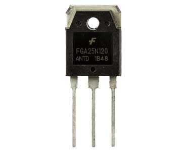
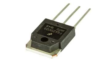
IGBT packages
IGBTs can be bought in a variety of formats. They are available as standard semiconductor devices, often in TO247, TO220, etc style packages or similar as well as surface mount packages such as SC-74, SOT-457 and many others. In view of the large switching capabilities of many IGBT devices, they tend to come in the larger packages.
IGBTs are also available in module formats. These IGBT modules are an assembly or module that contains several IGBT devices. They may be connected in one of several configurations such as a half-bridge, 3-level, dual, chopper, booster, etc.
Using a module enables a pre-designed item to be installed in a larger electronic design to provide a function without the need to develop the individual electronic circuits. They may also be more cost effective as the modules can be mass produced by the module manufacturer.
IGBTs, insulated gate bipolar transistors provide an additional component for the electronic circuit design of many power systems. By providing properties that combine some aspects of both bipolar transistors and MOSFETs, they are able to fill a niche in the electronic circuit designers toolbox that no other component is able to.
 Written by Ian Poole .
Experienced electronics engineer and author.
More Electronic Components:
Batteries
Capacitors
Connectors
ADC
DAC
Diodes
FET
Inductors
Memory types
Phototransistor
Quartz crystals
Relays
Resistors
RF connectors
Switches
Surface mount technology
Thyristor
Transformers
Transistor
Unijunction
Valves / Tubes
Return to Components menu . . .