What is a Silicon Carbide MOSFET
Silicon carbide, SiC MOSFETs are being widely used within many power applications where they provide a significantly improved level of performance over other technologies available.
Home » Electronic components » this page
FETs, Field Effect Transistors Includes:
FET basics
FET specifications
JFET
MOSFET
Dual gate MOSFET
Power MOSFET
MESFET / GaAs FET
HEMT & PHEMT
FinFET technology
IGBT
IGBT vs MOSFET - which is better?
Silicon carbide, SiC JFET
Silicon carbide, SiC MOSFET
Silicon carbide vs silicon MOSFETs
GaN FET / HEMT
SiC vs GaN
FET component data:
MOSFETs
SiC MOSFETs
GaN FETs
IGBTs
Silicon carbide is a semiconductor that is being used in an increasing number of electronic components. One good example of these is silicon carbide MOSFETs, often just referred to as silicon carbide FETs.
These silicon carbide, SiC MOSFETs or SiC FETs provide some useful improvements in performance over their silicon equivalent electronic components.
In essence these SiC MOSFETs provide a higher blocking voltage, lower on state resistance and higher thermal conductivity than their silicon counterparts.
This means that they are often using to good effect in electronic circuit designs for power switching: switch mode power supplies, voltage converters: step up and step down converters and many more electronic circuit designs.
Although there was initially a price penalty for using these devices, they are now so widely used and the manufacturing processes are so well established that there is little difference, and any cost increases associated with these electronic components can normally be more than made up because of the benefits resulting in smaller circuits, lower heat dissipation and the like.
What is silicon carbide
Silicon carbide may not normally be associated with semiconductor devices, but surprisingly it has been used for many years. In the days of crystal radio sets back in the 1920s and even a bit earlier in some cases, silicon carbide or carborundum as it was known, was used with Cat's Whisker radio detectors. These then became the first widely used silicon carbon or SiC diodes.
Silicon carbide is produced at high temperature combining silica - a form of silicon with carbon. This is refined and then processed to provide the required blanks on which the silicon carbide devices are formed. These electronic components may be SiC diodes, SiC FETs or SiC MOSFETs, etc.
Silicon carbide is now being widely used as the semiconductor for many power devices, because of its particular attributes. One key one is the very high breakdown electric field strength and this enables the fabrication of higher voltage semiconductor devices and in particular SiC MOSFETs.
Silicon carbide also possesses a number of other important attributes which mean that it performs particularly well within MOSFETs.
Note on Silicon Carbide:
Silicon carbide is a material that is known for its hardness, but it is also being used as a semiconductor providing devices that are able to offer new levels of performance, especially within power electronics designs.
Read more about Silicon Carbide.
Adoption of SiC MOSFETs
Silicon carbide technology did not find instant uptake like many other similar new inventions. It took time for the SiC technology to be developed and then adopted.
Although silicon carbide has been used within electronics for many years - crystal radio detectors in the 1920s and even earlier used carborundum which is silicon carbide as the "crystal" for detecting radio signals.
In fact it was using one of these crystals that H J Round, the British engineer first observed the light emitting diode effect, although he did not understand it.
Accordingly silicon carbide was known to be a semiconductor, but the processing techniques required for it took some while to develop. Silicon carbide is nowhere near as easy to process as silicon.
For the technology to become viable, it not only had to work, but the costs needed to make it competitive.
It was the fabrication costs that limited the adoption of SiC technology for many years. Substrate costs were much higher than those of equivalent silicon devices. The basic characteristics of the material itself and the high defect density meant that SiC MOSFETs and SiC diodes were not viable for many years.
Although it took a number of years to develop SiC technology to the level that was required for viable commercialisation, the processing of SiC for electronic components is now at the state where the defect density levels have been reduced and the processing costs have come down.
Accordingly it was in January 2011 that Cree introduced the first SiC MOSFET - the device known as the CMF20120D was specified at 1200V, had 80 mΩ ON resistance, and it was housed in TO-247 package.
This milestone launch meant that a viable SiC MOSFET was available, even though it cost more than a comparable IGBT. However its superior performance in terms of faster switching, higher efficiency and better thermal performance meant that many companies used in in their new electronic circuit designs.
Development of SiC technology has moved on and many more companies have introduced MOSFETs using silicon carbide as the semiconductor and next generation devices have also been developed providing a far higher level of performance.
Advantages of SiC MOSFETs
The use of silicon carbide MOSFETs is well established, particularly within the area of power electronics where the switching characteristics of these electronic components mean that they are particularly suited to many new electronics circuit designs.
Some of the key attributes of SiC MOSFETs arising from the use of silicon carbide rather than silicon include:
High voltage breakdown: Silicon carbide has a critical breakdown strength that is 10 times of silicon. This means that smaller and higher voltage SiC MOSFETs can be fabricated. Some SiC MOSFETs have operating voltages of well over 1.5kV, which is a figure well above that which can be achieved using silicon technologies.
The higher breakdown voltage enables the high breakdown voltages to be achieved whilst also using thinner drift layers.
Current density: SiC MOSFETs provide a much higher current density than silicon MOSFETs.
High temperature operation: Silicon carbide MOSFETs can operate at much higher temperatures than their silicon equivalents. This means that they can utilise the higher current density that SiC offers without the need for having to be so aware of the actual device temperature.
Low switching losses: Silicon carbide technology enables these MOSFETs to have a lower ON resistance. This results in lower resistive losses when the device in ON.
Also the faster switching speeds that can be attained mean that there is a faster transition between the ON and OFF states, which again results in lower loss levels.
The lower loss can be crucial in electronic circuit designs like voltage converters, switch mode power supplies and the like.
High switching frequencies: One of the parameters which can be particularly important with silicon carbide MOSFETs is the higher switching speeds that can be attained. This enables higher frequencies to be used, and this reflects in smaller inductive and capacitive components being needed. Not only does this reduce the size of the overall electronic circuit design, but it also reduces costs as smaller electronic components cost less.
SiC MOSFET circuit design considerations
SiC MOSFETs are now tending to dominate a number of areas of electronic circuit design, especially within a number of areas of power supply electronics design.
The fundamental operation of SiC FETs is very similar to that of the more traditional silicon based MOSFETs, but there are a few design considerations that need to be taken into consideration.
In many instances the circuit may need a few alterations, although soem other aspects may require a little more attention to ensure the correct operation of the electronic circuit design.
- Gate drive requirements: One of the main areas where SiC MOSFETs differ from their silicon counter parts is with the gate voltage requirements.
These devices require a higher gate-to-source voltage to achieve the lowest VDS saturation voltage at high drain current levels. Most silicon MOSFETs achieve low VDS saturation of around 8 V to 10 V between the gate and source. However SiC MOSFETs typically require 15 V to 20 V VGS to achieve low VDS saturation. This means that the electronic circuit design needs to be tailored to suit this.
Specific SiC MOSFET gate driver ICs are available to provide the required gate signals and at the right voltages. These are an ideal way of ensuring the required gate drive is developed for any SiC FET electronic circuit design.
- Isolation between input and output: Because SiC MOSFETs are used for many power switching applications, this means that it is necessary to have isolating transformers between the input and output. This is undertaken on the input where the switching signals can be passed through a transformer.
- Electromagnetic interference, EMI: The very much faster switching of SiC MOSFETs when compared to other devices - IGBT, power MOSFETs, etc, means that much higher frequencies are present from the switching. These high frequencies can give rise to electromagnetic interference. As a result this must be considered within the electronic circuit design of any system using these electronic components.
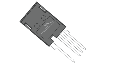
- Additional source pin: Although many SiC MOSFETs have three connections like any other MOSFET, some have an extra connection which might be confusing at first sight.
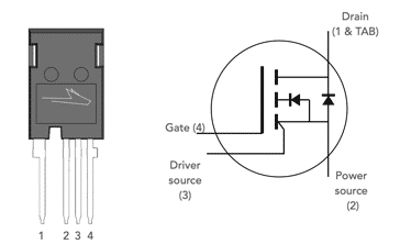
Connections for a typical SiC MOSFET showing the Kelvin sourcepin As can be seen from the diagram the gate and drain are present as normal, but there are two connections for the source. One is labelled driver source and the other power source. The additional source pin associated wit the input circuitry is sometimes referred to as a Kelvin source pin.
The reason for this is to keep the input circuitry as isolated as possible from the output. Even short lead lengths could introduce significant issues because of the levels of current and the switching speeds that are commonplace with these designs.
If the gate driver is referenced to the same ground that carries the load current, then even small values of series resistance and inductance could cause switching spikes to be experienced by the input. Separating them out will provide some degree of additional isolation. In some ays it is a little like separating the load and sense wires in a high current power supply.
The additional pin, known as the Kelvin source pin is taken as close to the source as possible on the semiconductor die and the connection extracted separately to reduce any effects of stray inductance and resistance that might cause issues with the drive circuitry.
- RDS(ON) variance with temperature: One significant factor with SiC MOSFETs is the low RDS(ON) figure and the fact that it changes by a fact which can be as little as 1.3 to 1.4 over the operating temperature range. By contrast, silicon and even GaN devices may exhibit RDS(ON) figures that may double or triple when temperatures rise from 25°C to the maximum which may be around 140°C. But check the data-sheets for exact figures.
- High VDS specification: The high breakdown voltages associated with SiC FETs can bring many dividends in the electronic circuit design of various items, especially for power supply applications: switch mode power supplies, voltages converters and power control, etc.
Although IGBTs are typically rated around 1.2kV and many SiC MOSFETs may have a similar rating (although many have even higher VDS ratings), the actual final breakdown of the silicon carbide electronic component will be much higher, enabling a very high degree of derating to be incorporated into the circuit which would not be possible with an IGBT or standard power MOSFET. The SiC electronic components are able to withstand much higher levels of transients, and these are present in all power systems from time to time.
- Reverse recovery time: Reverse recovery time is an important aspect of switching circuits, especially those used in symmetrical designs. Electronic circuit designs for voltage converters including buck and boost circuits as well as power correction circuitry. SiC MOSFETs have a reverse recovery time of ten measured int he low tens of nanoseconds whereas equivalent high voltage silicon MOSFETs may have times of around three quarters of a millisecond. The fast reverse recovery time of SiC MOSFETs can be utilised to increase the speed of operation, e.g. the switching speed of a switch mode power supply, etc and this results in smaller inductors and capacitors being needed, and in turn this means efficiency can be improved whilst significantly lowering the costs of the electronic components in these circuit designs.
SiC switching modules
In addition to the basic SiC MOSFETs themselves, a number of companies provide SiC switching modules. These SiC modules provide all the circuitry required for provide the switching needed from a low level input.
These SiC modules will ensure the right drive requirements for the MOSFET are provided as well as looking at the snubber circuitry and EMI filtering that will be needed within the overall electronic circuit design.
These SiC modules are ideal for many circuit designs where an effective module is needed and standard drive levels are available, etc. They can provide a very cost effective solution because they reduce design time and from the economies of scale of producing a large number of modules for a variety of customers, they will often often offer a lower material or electronic component cost than if a switcher had been designed internally for the specific system
SiC MOSFETs and in general silicon carbide technology has enabled semiconductor performance for many applications to be moved forward in almost a quantum leap. The performance of silicon carbide MOSFETs gives some significant improvements when compared to existing technologies such as silicon MOSFETs and IGBTs.
While it is always wise to look at all the alternatives including electronic components like power MOSFETs (VMOS, HEXFETs, UMOS, etc) and IGBTs, SiC MOSFETs are able to provide an ideal solution for many new electronic circuit designs.
 Written by Ian Poole .
Experienced electronics engineer and author.
More Electronic Components:
Batteries
Capacitors
Connectors
ADC
DAC
Diodes
FET
Inductors
Memory types
Phototransistor
Quartz crystals
Relays
Resistors
RF connectors
Switches
Surface mount technology
Thyristor
Transformers
Transistor
Unijunction
Valves / Tubes
Return to Components menu . . .