Pi & T Resistive Attenuator Pads: RF Circuit Design
The RF circuit design for resistive Pi and T attenuator pads is easy and the formulas calculations and circuits are very straightforward.
Home » Radio & RF technology » this page
RF Attenuators Includes:
Attenuator basics
Attenuator specs
Resistive attenuator design
Attenuator resistor values table
Balanced resistive attenuator pads
Variable PIN diode attenuator
SMA attenuator
RF resistive attenuator pads are used in many RF circuit design applications. The RF circuit design for resistive attenuator pads is very easy and they can be incorporated into many RF circuits very easily.
RF attenuators reduce the level of the signal and this can be used to ensure that the correct radio signal level enters another circuit block such as an RF mixer or amplifier so that it is not overloaded, and they are also used to ensure that a good impedance match is obtained.
Either Pi or T attenuator pads can be used and there is little to choose between them. They both use the same number of electronic components. Bridge T attenuator pads can also be used if required, but whilst they have some advantages in specific RF design applications, further electronic components are needed.
If the correct components and circuit techniques are used, then these attenuator pads can easily be used to operate at frequencies well into the GHz region. Surface mount technology resistors are particularly good, and modern PCB technology provides a good base for frequencies well above 1 GHz, although care may need to be taken when choosing the PCB material as some may be lossy and give the incorrect performance.
Resistive attenuator pad types
There are several RF design formats for resistive attenuators. All perform equally as well, but sometimes there may be different reasons or preferences for selecting a particular type or format for a particular RF circuit design application.
The main formats for RF resistor attenuator circuits are summarised below:
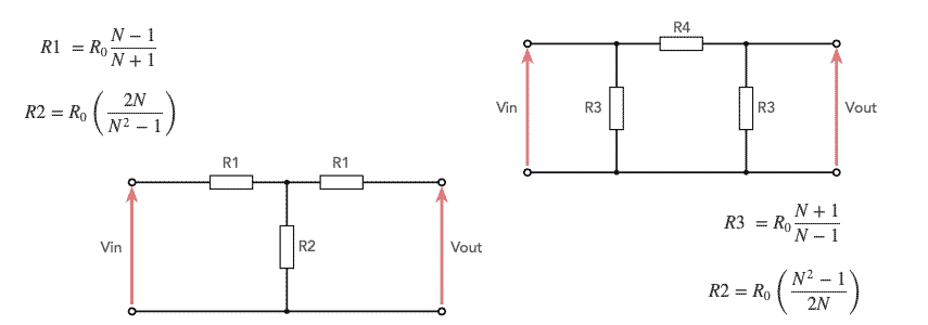
Pi attenuator pads: As the name indicates the pi attenuator pad has a topology similar in shape to the letter Π. This RF attenuator format has a single series resistor in the signal line between the input and output connections and then at both the input and output a resistor is taken to ground.
By selecting the right values for the resistors, it is possible to achieve the required level of attenuation as well as having the required characteristic impedance. In fact this characteristic impedance should be as purely resistive as possible for most RF circuit design applications.
- T attenuator pads: In terms of topology the T attenuator pad (or Tee attenuator pad) is the opposite of the Pi section resistive attenuator, but it performs equally as well. This form of RF attenuator has two resistors in series with each other between the input and the output. A single resistor is taken to ground from the junction of the two series resistors. In this way the series resistors on the input and output, forming a T section.
- Bridged T attenuator pads: The bridged T attenuator can be thought of as a combination of the Pi and T attenuator pad topologies. This for of RF attenuator uses more electronic components, but still provides the impedance match and attention levels needed for most attenuator applications within an RF circuit design.
Both the Pi attenuator pad format and the T attenuator pad format perform equally well. Often the preference of which type to use is a matter of personal preference for the designer.
Normally the RF design requires that the same impedance is seen at both input and output, but it is possible to design the sections so that they have different input and output resistance / impedance levels if required.
T attenuator pad format
The diagram below shows the format for the T attenuator pad format. As the name implies, the T attenuator pad is in the form of a letter T with two resistors in series in the signal line and a single resistor to ground at the junction of the two series resistors.

Assuming the same input and output impedance levels are the same, the two resistor values can be calculated very easily knowing the ratio of the input and output voltages, Vin and Vout respectively and the characteristic impedance Ro.
Pi attenuator pad format
The pi attenuator pad topology is in the form of the Greek letter pi and has one in line resistor and a resistor to ground at the input and the output.
The basic RF attenuator section consists of three resistors and as such needs very few electronic components.

Similarly the values for the pi section attenuator pad can be calculated:
Bridged T attenuator
The bridged T attenuator can be used in a number of RF design scenarios for which it provides some distinct advantages.
The bridged T attenuator can be thought of as a modified Pi attenuator. There is one resistor in line and two, one at either end that connect to a common junction point that passes signal to earth via a fourth resistor.

The bridged T attenuator pad is often the favoured format for variable RF attenuators, especially those using PIN diodes. The reason for this is that the bridged T attenuator pad only requires the use of two variable resistors against the three required for both the Pi and T attenuator pads.
A further advantage is that as the bridged T attenuator pad has a tendency to match itself to the characteristic impedance Zo. At high attenuation levels R5 is at a high resistance and R6 is low. Accordingly the predominant resistor values at those labelled R which is equal to the characteristic impedance.
RF attenuator design considerations
When undertaking the RF design of an attenuator there are several points that should be considered if the best performance is to be achieved.
A few simple Rf design guidelines can ensure that the performance of the attenuator meets its requirements
Components: The choice of electronic components used in the attenuator construction can have a major impact on the performance. By using the correct components in the attenuator construction, it is possible to obtain high performance levels.
One of the key requirements is to ensure that non-inductive resistors are used. Surface mount resistors are particularly good, because they are small and are not manufactured using any spiral cutting techniques. Accordingly the levels of stray inductance are very low.
In terms of conventional electronic components a variety of forms of resistor are available. Wire-wound resistors are obviously not acceptable because of their high levels of inductance, but as many other types use spiral cutting techniques to trim the resistance levels, some level of inductance may be introduced. This may introduce some stray effects at higher frequencies, although at frequencies, certainly below 30 MHz most types should operate satisfactorily. Specialised non-inductive resistors can be obtained where higher frequency operation, flat frequency responses and accurate levels of attenuation are needed.
Surface mount technology resistors are particularly good because their small size and lack of leads means that they exhibit very low levels of inductance. However when using surface mount resistors, care needs to be taken to ensure they have sufficient power handling capacity.
Attenuator sections: One key element of attenuator construction and design, is not to attempt to achieve a very high level of attenuation in one stage. If high levels of attenuation are attempted in a single stage, then the stray effects such as inductance, capacitance and imperfections in earthing may lead to the signal effectively bypassing the attenuator itself and the required level of attenuation not being accurately achieved.
If high levels of attenuation are required, then it is far better to build the attenuator in several sections - cascading several sections - so that the overall level of attenuation is achieved in stages. In this way the stray effects are not as significant
In attenuator construction, it is generally good practice not to attempt to achieve any more than a maximum of 20 dB attenuation in any one attenuator section. When this is done the adjoining resistors can be combined. In the case of the T section attenuator this simply means the two series resistors can be added together. For the Pi section attenuators there are parallel resistors.
Stray capacitance: There can be very small amounts of stray capacitance that occur between elements of the circuit. These can significant levels in terms of performance, especially when they occur between the input and output of the attenuator. The result is that the input and output of the attenuator, or other areas are bypassed, especially at high frequencies. In view of this it is necessary to ensure that the input and output are kept sufficiently far apart and that capacitance between them is minimised.
Add screening between sections: It is worth considering whether to add screening between the different sections. If there is a possibility of capacitive coupling, then screens might help ensure the required level of attenuation is achieved.
Stray inductance: When building an attenuator, any leads can provide a path for inductive coupling. Like the capacitance, this is particularly important in terms of coupling the input to the output.
Poor earthing: As attenuation levels rise, the importance of the earthing increases. Levels of resistance can result in signal leakage around the attenuator.
Power dissipation: Some attenuators need to dissipate medium to large levels of power. The signal that is lost needs to have its power dissipated within the resistors. For signal level RF designs, this is not an issue in most instances, although transient may be an issue. The resistors need to be selected to ensure that they can dissipate the expected levels of power, with soem spare margin as well. Also for long term reliability it is necessary to ensure resistors the power handling capacity of the resistors has a reasonable margin over what might be expected, and temperature rises within the resistors is kept within acceptable boundaries for the electronic components used.
Buy Your Concise Guide to RF Attenuators:
This downloadable PDF concise guide provides all the basics you need to understand about constant impedance Pi and T RF attenuators and their design. It is a really great guide packed with information.
Buy your download now PDF downloadable 'Concise Guide to RF Attenuators & Their Design.
RF attenuators information infographic
In order to summarise the basics of the more popular circuits and their design information, I've prepared a summary infographic.
This gives the circuits for the Pi and T section attenuators along with their design equations.
There's also a table of resistor values for the more commonly usd attenuation levels so there's no need to calculate everything.
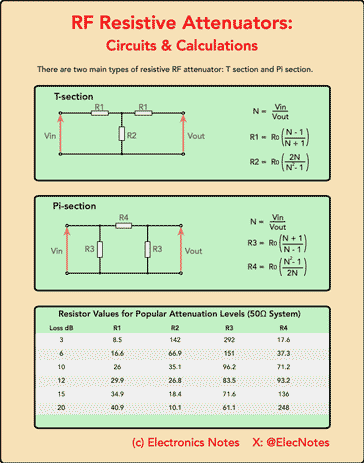
Click on image for larger version
In many respects there is little difference between the pi and t attenuator pads. The choice of which type of pad to use often results from the preference of the design engineer. It may even result from the convenience of the values that result from the calculations. If the values from one type of attenuator pad fall conveniently close to standard values or those already in a design, then this may be a good reason for choosing "Pi" rather than a "T" attenuator pad or vice versa.
 Written by Ian Poole .
Experienced electronics engineer and author.
More Essential Radio Topics:
Radio Signals
Modulation types & techniques
Amplitude modulation
Frequency modulation
OFDM
RF mixing
Phase locked loops
Frequency synthesizers
Passive intermodulation
RF attenuators
RF filters
RF circulator
Radio receiver types
Superhet radio
Receiver selectivity
Receiver sensitivity
Receiver strong signal handling
Receiver dynamic range
Return to Radio topics menu . . .

