FET Circuit Configurations Explained
Understanding FET circuit configurations is at the heart of FET circuit design - common source, common gate & common drain formats each have their own characteristics.
FET, Field Effect Transistor Circuit Design Includes:
FET circuit design basics
Circuit configurations
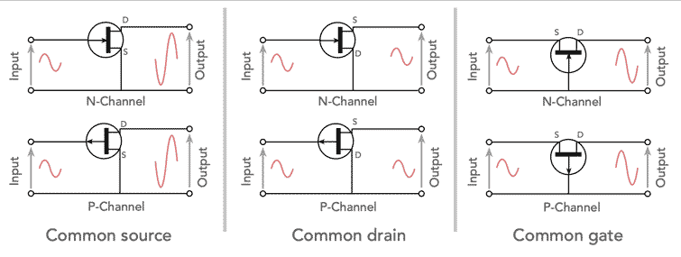
Common source
Common drain / source follower
Common gate
When designing circuits using field effect transistors there are various circuit configurations, and in fact these mirror those used with bipolar transistors and the older vacuum tubes / thermionic valves.
FET circuit configurations are the common source, common gate, and common drain formats. Each have their own characteristics of voltage and current gain as well as input and output impedance.
The choice of the FET circuit configuration or topology is one of the key design parameters on which the overall circuit design is based.
FET configuration basics
The terminology used for denoting the three basic FET configurations indicates the FET electrode that is common to both input and output circuits. This gives rise to the three terms: common gate, common drain and common source.
There are three different configurations, each with different characteristics. We'll look at them in turn: common source, common drain, common gate:/p>
• Common source
This FET configuration is probably the most widely used. The common source circuit provides a medium input and output impedance levels.
Both current and voltage gain can be described as medium, but the output is the inverse of the input, i.e. 180° phase change.
This provides a good overall performance and as such it is often thought of as the most widely used configuration.

• Common drain
This FET configuration is also known as the source follower. The reason for this is that the source voltage follows that of the gate.
Offering a high input impedance and a low output impedance it is widely used as a buffer. The voltage gain is unity, although current gain is high.
The input and output signals are in phase.

• Common gate
This transistor configuration provides a low input impedance while offering a high output impedance.
Although the voltage is high, the current gain is low and the overall power gain is also low when compared to the other FET circuit configurations available.
The other salient feature of this configuration is that the input and output are in phase.

FET circuit configuration summary table
It's important to have an understanding of the key characteristics of each configuration as these enable the right configuration to be selected for the particular circuit design.
The table below gives a summary of the major properties of the different FET circuit configurations.
| FET Configuration Summary Table |
|||
|---|---|---|---|
| FET Configuration | Common Gate | Common Drain (Source follower) |
Common Source |
| Voltage gain | High | Low | Medium |
| Current gain | Low | High | Medium |
| Power gain | Low | Medium | High |
| Input resistance | Low | High | Medium |
| Output resistance | High | Low | Medium |
| Input / output phase relationship | 0° | 0° | 180° |
As can be seen the different configurations or topologies have different characteristics. The common source is the most widely used FET circuit configuration and it equates to the common emitter transistor amplifier. The FET common drain or source follower is used as a buffer amplifier and it equates to the transistor common emitter amplifier.
 Written by Ian Poole .
Experienced electronics engineer and author.
More Circuits & Circuit Design:
Op Amp basics
Op Amp circuits
Power supply circuits
Transistor design
Transistor Darlington
Transistor circuits
FET circuits
Circuit symbols
Return to Circuit Design menu . . .