
Op Amp Specifications & Datasheet Parameters
Understand the datasheet parameters and specifications for operational amplifiers so that the right op amp can be selected.
Op-amp Tutorial Includes:
Introduction
Op amp gain
Bandwidth
Op amp slew rate
Offset null
Input impedance
Output impedance
Current feedback op amp
Understanding specifications
How to choose an op amp
Op amp circuits summary
Understanding what the op amp specifications mean that are written in the datasheets is key to knowing what performance they will provide and selecting the right op amp for any particular electronic circuit.
Like any electronic component, operational amplifiers have their performance defined in datasheets - these carry a variety of specifications and parameters which define the performance, and from these it should be possible to identify whether any given device will be suitable for a particular application.
Some op amps are ideal for general applications, whereas other op amp chips have been designed to provide particular levels of performance in some areas. Chips designers have to balance cost, and various conflicting areas of performance and therefore it is not possible to provide a single chip that meets every single requirement.
The table below provides details of some of the major specifications and parameters encountered in op amp datasheets.
| Common Op Amp Specifications & Datasheet Parameters | ||
|---|---|---|
| Spec | Op amp Specification / Parameter Details | |
| φm | Phase margin | This specification is absolute value of the open-loop phase shift between the output and the inverting input at the frequency at which the modulus of the open-loop amplification is unity. |
| Am | Gain margin | This parameter is often seen in datasheets and is the reciprocal of the open-loop voltage amplification at the lowest frequency at which the open-loop phase shift is such that the output is in phase with the inverting input. |
| AV | Large signal voltage amplification | This parameter is one of the commonly used specifications. It is the ratio of the peak-to-peak output voltage swing to the change in input voltage required to drive the output for large signals. |
| AVD | Differential voltage gain | This parameter is the ratio of the change in the output voltage to the change in differential input voltage producing it with the common-mode input voltage held constant. i.e. this is the gain for a voltage difference between the inverting and non-inverting inputs. |
| Unity gain bandwidth | This parameter is the bandwidth for which the open-loop voltage amplification is greater that unity, i.e. the frequency at which the gain falls to unity. | |
To help your home lab or workshop . . . . . .
To help you with your home workshop or radio shack, etc, we thought these might help:

85PCS 10 Types NE555 LM324 LM393 UA741 ULN2803 LM358 LM386 NE5532 ULN2003 PC817 Integrated Circuit DIP IC Kit
This kit is ideal for home workshops and electronics labs as it provides a good selection of operational amplifiers, op-amps, and other useful integrated circuits.

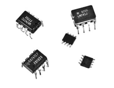
10PCS UA741CN 741 operational amplifier DIP-8
The 741 is possibly the most famous operational amplifier. Even today, it is a great "jelly bean" chip that is a great general purpose IC, which is widely available and very cheap.

LM358 Surface Mount SOIC-8 Low Power Dual Operational Amplifier choice of 5 or 10 pcs
The LM358 is a well known and used Op-Amp. This version is in a surface mount SOIC-8 package and is available in either 5 or 10 pcs.
A Guide to Operational Amplifiers and Their Circuits
Written by Ian Poole, this PDF downloadable ebook gives a great introduction to operational amplifiers: what they are, how they work, some circuits with design calculations, hints and tips . . . . in fact all you need to know to get started.
Check out more items you might like from my Components store.
More convenient to buy from Amazon.com? Check out Op-Amps on my Amazon Storefront.
Note: We make a small commission from any sales at no cost to you.
| Common Op Amp Specifications & Datasheet Parameters | ||
|---|---|---|
| Spec | Op amp Specification / Parameter Details | |
| Ci | Input capacitance | This is the capacitance between the input terminals with either input grounded. |
| CMMR | Common mode rejection ratio | This is a particularly important parameter or specification for applications where the differential amplification only is needed. This might be needed for low signal applications where a differential drive is used to reduce common mode noise pick up. CMMR is the ratio of differential voltage amplification to common-mode voltage amplification. This is measured by determining the ratio of a change in input common-mode voltage to the resulting change in input offset voltage. |
| GBW | Gain bandwidth product | This op amp specification parameter is the product of the open loop voltage gain and the frequency at which it is measured. |
| ICC+, ICC- | Supply current | This specification parameter represents the supply current into the VCC+ or VCC- terminals of the op amp integrated circuit, i.e. the positive and negative supply rail current levels. |
| IIB | Input bias current. | As the input transistors of the op amp require bias, a certain current, however small is required for them to operate. This specification details the amount of current required and it is defined as the average current into the two input terminals with the output at a given level. |
| IOL | Low level output current | This parameter defines the output current the device can supply. Maximum figures will be given in the specification and these should not be exceeded. Above the limits the current will limit. |
| PD | Total power dissipation | This is the total power dissipation in the device and is equal to the power delivered into the device, less any delivered to the load. The power dissipation maximum should not be exceeded otherwise the device will become too hot and this can damage the device. Operating at high temperatures is known to increase failure rates. |
| ri | Input resistance | This specification parameter is the resistance between the two input terminals of the op amp with one terminal grounded. |
| rid | Differential input resistance | This parameter is the small signal resistance between two ungrounded input terminals of the op amp. |
| ro | Output resistance | This is the output resistance of the op amp device measured between the output terminal and ground. Note that even though the device will have a low output resistance its current drive capability is limited and will not enable it to drive low impedance loads. |
| SR | Slew rate | This is the time taken for the output to change for a given input. As the output is unable to fully follow the input waveform and its speed is limited there is a maximum rate at which it can change. The slew rate parameter is normally quoted in volts per µs or sometimes volts per ms for op amps. |
| THD+N | Total harmonic distortion plus noise | This specifications defines the ratio of the RMS noise voltage and the RMS harmonic distortion in volts of the fundamental signals to the total RMS voltage at the output. It represents the total of the unwanted products at the output. As a ratio, it is normally expressed as a figure in dB. |
| Vi | Input voltage range | This is the voltage range over which the operational amplifier can operate. If this parameter is exceeded then it can cause the op amp to malfunction or it can cause damage. |
| VIO | Input offset voltage | This parameter is the DC voltage that must be applied between the input terminals to provide a DC output voltage of zero. If both inputs were grounded, the output voltage of the op amp would not be zero - there is a small offset. This offset can be an issue with circuits requiring accurate DC voltages. |
| Vn | Equivalent input noise voltage | All op amps generate some noise. This specification parameter defines the noise performance of the op amp. It is the voltage of an ideal voltage source placed in series with the input terminals that represents the internally generated noise. |
| VOM | Maximum peak output voltage swing | This op am specification parameter is the maximum positive or negative output voltage that can be obtained without the waveform clipping and when the DC quiescent voltage is zero. |
| VO(PP) | Maximum peak-to-peak output voltage swing | This is the maximum peak to peak voltage that can be obtained without waveform clipping with a DC quiescent voltage of zero. |
| Zic | Common mode input impedance | As the input of an op amp is not only resistive, it is often more convenient to consider the input impedance. This parameter is the sum of the small signal impedance between each input terminal and ground. |
| Zo | Output impedance | Like the input circuitry of the op amp, the output is also complex and this parameter represents the small signal impedance between the output terminal and ground. |
Understanding what these specifications mean, will help make the selection of the right op amp for the given application or circuit - like any other component, careful consideration is required to ensure that the optimum choice is made, although often the various specifications may need to be balanced to obtained the right electronic component for the job.
These are some of the more important and widely used op amp specifications that will be seen mentioned in the datasheets showing all the different parameters of the op amps.
Whilst it is often possible and quite acceptable to choose a low cost general purpose op amp, there are some instances where better performance may be required, and a higher performance op amp may need to be selected. Understanding the specifications enables the right choice to be made.
 Written by Ian Poole .
Experienced electronics engineer and author.
Essential operational amplifier data:-
Make your op-amp selection with op-amp data as well as distributor price and availability.
Check it out now!
More Circuits & Circuit Design:
Op Amp basics
Op Amp circuits
Power supply circuits
Transistor design
Transistor Darlington
Transistor circuits
FET circuits
Circuit symbols
Return to Circuit Design menu . . .


