Common Base Transistor Amplifier
The common base amplifier configuration is not widely used except in high frequency amplifiers where it has some distinct advantages.
Transistor Circuit Design Tutorial Includes:
Transistor circuit design
Circuit configurations
Common emitter
Common emitter circuit design
Emitter follower
Common base
See also:
Transistor circuit types
The common base amplifier is the least widely used of the three transistor amplifier configurations. The common emitter and common collector (emitter follower) configurations are far more widely used because their characteristics are generally more useful.
However, the common base amplifier configuration comes into its own in a number of circumstances where a low input impedance are needed.
This circuit configuration also offers a low input and medium to high output impedance level and it lends itself to a number of RF circuit design applications where 50Ω input impedance levels are needed.
This means that even though it is not used for many run-of-the-mill electronic circuit designs, it can be a very useful option where some of its key characteristics can be used.
Common base transistor amplifier basics
The common base amplifier has a rather different style of configuration to that of the other electronic circuit design configurations.
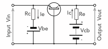
Normally the signal input is applied to the base, but in the case of the common base, this connection is grounded and in fact it is occasionally called a grounded base circuit design.

For both NPN and PNP circuits, it can be seen that for the common base amplifier circuit, the input is applied to the emitter, and the output is taken from the collector. The common terminal for both circuits is the base.
The base is grounded for the signal although for biassing reasons, the DC potential will be above ground level. Tis is achieved using DC bias resistors but decoupling the base to ground using a capacitor.
The common base amplifier configuration is not used as widely as transistor amplifier configurations. However it does find uses with amplifiers that require low input impedance levels. One application is for moving-coil microphones preamplifiers - these microphones have very low impedance levels.
Another application is for RF circuit designs within VHF and UHF RF amplifiers where the low input impedance allows accurate matching to the feeder impedance which is typically 50Ω or 75Ω.
The configuration also improves stability as a result of the base being grounded and this can give rise to the amplifier being called a grounded base amplifier on some ocasions.
With the base being the electrode that is between the emitter and collector, the fact that it is grounded for RF signals reduces the level of unwanted spurious feedback int he circuit design.
It is worth noting that the current gain of a common-base amplifier is always less than unity.
However the voltage gain is more, but it is a function of input and output resistances (and also the internal resistance of the emitter-base junction). As a result, the voltage gain of a common-base amplifier can be very high.
Common base transistor amplifier characteristics summary
The table below gives a summary of the major characteristics of the common base transistor amplifier.
| Common base characteristics |
|||
|---|---|---|---|
| Parameter | Characteristics | ||
| Voltage gain | Medium | ||
| Current gain | Low | ||
| Power gain | Low | ||
| Input / output phase relationship | 0° | ||
| Input resistance | Low | ||
| Output resistance | Medium to high | ||
The common base circuit does not find many applications for low frequency circuits - normally a high input impedance and low output impedance are desirable. However, it is occasionally used for some circuits that require a low input impedance such as that for a ribbon microphone and a few other electronic circuit design situations.
Where it does find some uses is within RF design for some high-frequency amplifiers, for example for VHF and UHF, etc.
In the common base configuration the input capacitance does not suffer from the Miller effect, which degrades the bandwidth of the common-emitter configuration. Also there is a relatively high isolation between the input and output and this means that there is little feedback from the output back to the input, leading to high stability.
How does the common base circuit work
In terms of the signal flow, the common base circuit is rather different to that of either the common emitter or common collector / emitter follower circuit design.
As the other two circuit designs use the base electrode as the input point of the circuit, the same cannot be true for the common base circuit design as it is grounded.
This circuit design uses an NPN transistor, but the configuration is equally applicable to PNP transistors but with battery polarities reversed.
Common base transistor amplifier circuit
The diagram below shows how a common base amplifier circuit can be implemented. It shows a very standard configuration for the electronic circuit design for the bias as well as the application of the signals to the circuit.
The same bias constraints apply to the common base circuit, but the application of the signals is different, allowing the base to be earthed and hence common to both input and output circuits.

In this typical electronic circuit design for a common base transistor amplifier, the bias conditions are very similar to those used to bias other forms of configuration such as the common emitter
In terms of the electronic circuit design, the resistors R1 and R2 form a potential divider which sets the bias point for the base. The emitter of the transistor will be 0.6 volts below this, assuming a silicon transistor is used.
The emitter resistor R4 determines the current flowing through the emitter resistor. As virtually the same current will flow through the collector, care must be taken to ensure that the resistor R3 is chosen such that the signal does not cause any limiting.
The capacitors C1 and C2 provide the AC coupling for the circuit and the values should be chosen so that their impedance is low at the frequencies of operation.
The values of R3 and R4 are likely to be influenced by the impedance required for the system. If low values are chosen for these resistors, then it will affect the current that needs to flow within the circuit.
RF amplifier
there are diferent requirements for some RF circuits and the common base circuit has been re-drawn and different components used to provide the required RF performance.
Even here, the circuit components may be altered to suit the actual requirements for the circuit. RFC2 may be an RF transformer, as might RFC1.

Although the common base transistor circuit is not as widely used as either the common emitter or common collector / emitter follower circuit designs, it nevertheless has its place within the electronic circuit design library. It uniquely has a low input and output impedance and is able to provide improved stability at high frequencies as a result of the base being grounded.
In terms of the number of electronic components used, it is very similar to the other main circuit configurations.
 Written by Ian Poole .
Experienced electronics engineer and author.
Essential bipolar transistor data:-
Make your BJT transistor selection with op-amp data as well as distributor price and availability.
Check it out now!
More Circuits & Circuit Design:
Op Amp basics
Op Amp circuits
Power supply circuits
Transistor design
Transistor Darlington
Transistor circuits
FET circuits
Circuit symbols
Return to Circuit Design menu . . .