Transistor Common Emitter Amplifier
The common emitter amplifier configuration provides voltage gain and is one of the most widely used transistor configurations for electronic circuit design.
Transistor Circuit Design Tutorial Includes:
Transistor circuit design
Circuit configurations
Common emitter
Common emitter circuit design
Emitter follower
Common base
See also:
Transistor circuit types
The common emitter transistor amplifier circuit is one of the mainstay circuits for use within electronic circuit design offering many advantages.
The common emitter circuit configuration is used in many areas of electronic circuit design: as an audio amplifier, as a basic switch for logic circuits, as a general analogue amplifier and in many other applications.
The common emitter circuit configuration provides voltage gain combined with a moderate current gain, as well as a medium input and a medium output impedance. As such the common emitter configuration is a good all round circuit for use in many applications.
It is also worth noting at this stage that the common emitter transistor amplifier inverts the signal at the input. Therefore if a waveform that is rising enters the input of the common emitter amplifier, it will cause the output voltage to fall. In other words it has a 180° phase change across the circuit.
Dependent upon the actual electronic circuit design itself, the common emitter does not use too many electronic components, sometimes as few as two resistors, although if the bias needs setting for analogue circuits, then four resistors and three capacitors may be used.
Video: Understanding the Transistor Common Emitter Circuit Configuration
Common emitter transistor amplifier basics
Of the three types of transistor configuration used in electronic circuit design, the common emitter is the most widely used because of its key attributes.
The common emitter amplifier has the signal applied to the base and the output is then taken from the collector circuit. However, as the name of this circuit implies, the key attribute is that the emitter circuit is common to both input and output.

The common emitter configuration is equally applicable to both NPN transistor and PNP transistor variants. That said the NPN variety is more commonly used because of the more widespread us of NPN transistors.
Common emitter transistor amplifier characteristics summary
When selecting the transistor configuration to be used within an electronic circuit design, it is necessary to consider the various attributes of the three types: common emitter, common collector and common base, and select the one that is most appropriate.
The table below gives a summary of the major characteristics of the common emitter transistor configuration.
| Common emitter transistor amplifier characteristics |
|||
|---|---|---|---|
| Parameter | Characteristics | ||
| Voltage gain | Medium | ||
| Current gain | Medium | ||
| Power gain | High | ||
| Input / output phase relationship | 180° | ||
| Input resistance | Medium | ||
| Output resistance | Medium | ||
From these characteristics, it can be seen that the common emitter configuration provides good all round performance. One of e key factors is that it provides a good level of voltage gain, an attribute that is required in electronic circuit design for many applications.
The circuit is also relatively straightforward needing a few electronic components, dependent upon how the electronic circuit design requirements are fulfilled.
Common emitter amplifier impedance levels
One of the key attributes to be considered when undertaking any electronic circuit design are the impedance levels.
The input impedance is typically around 1kΩ, although this can vary considerably according to the circuit values and conditions. The low input impedance results from the fact that the input is applied across the base and emitter where there is a forward-biased junction,
Also the output impedance can be relatively high. Again this varies considerably upon the electronic component values chosen and current levels permitted. The output impedance may be as high as 10kΩ or possibly more. However if current drain allows higher current levels to be drawn, the output impedance can be reduced considerably. The level of resistance or impedance comes from the fact that the output is taken from the collector where there is a reverse-biased junction.
Common emitter transistor amplifier gain
Another important factor to be considered at the outset of the electronic circuit design is the gain level that can be achieved. There are two forms of gain that can be determined: current gain and voltage gain.
The current gain for the common emitter amplifier circuit is denoted by the Greek symbol β. This is the ratio of collector current to base current. This may be thought of as the ratio of output current to input current. To gain an accurate figure of the gain for a signal, the current gain for small input changes in current is often used. Using this the current gain, β, and the changes in input and output current are related in the following way:
Where
β = current gain
ΔIc = change in collector current
ΔIb = change in base current
In order to look at the voltage gain of the common emitter amplifier circuit, it is necessary to look at the resistances or impedances for the input and output.
Therefore:
Where
Av = voltage gain
Rc = collector circuit output resistance
Rb = base circuit input resistance
Common emitter input output phase relationship
The common emitter transistor amplifier is the only configuration that gives an inversion, 180°, between the input and output signals.
The reason for this can be seen from the fact that as the input voltage rises, so the current increases through the base circuit. In turn this increases the current thought the collector circuit, i.e. it tends to turn the transistor on. This results in the voltage between the collector and emitter terminals falling.
In this way an increase in voltage between the base and emitter has resulted in a fall in voltage between the collector and emitter terminals, in other words the phase of the two signals has been inverted.
Ideas for your projects . . . . . .
Products with great prices in association with AliExpress. But also don't forget my Amazon.com storefront.

50-900PCS Transistors kit: NPN PNP
A variety of transistors including S8050 S8550 S9012 2N3904 2N3906 C1815 A1015 MJE13001 BC327 BC337 BC517 BC547 BC548 BC549 BC558. Select the kit on ordering that gives you the required quantity and types.

100 pcs 2N2222 Transistor
The 2N2222 transistor is one of the classics of all time and even today it performs well and can be used in very many circuits - an ideal general purpose transistor

TIP41C TIP42C Bipolar Power Transistor (5pcs TIP41+ 5pcs TIP42)
The TIP41 and TIP42 are ideal power transistors which can used in a complementary power output stage.

10-30PCS 2N3055 Power Transistors NPN
The 2N3055 is a classic power transistor which even today performs well. With its 15A / 60V and mounted in a TO3 metal can it is a really great device.
. . More Transistors (BJTs) . . .
More convenient to buy from Amazon.com?
Note: We make a small commission from any sales at no cost to you.
Practical common emitter amplifier circuits
When undertaking electronic circuit design for various applications and to meet various requirements, it is possible to use one of a variety of variants of the common emitter transistor circuit.
While the basic theoretical circuits shown above are able to describe the basic operation of the common emitter amplifier in concept.
However, for the circuit to be able to operate in a real system, other elements such as bias, decoupling and the like need to be added. As a result, the overall circuit for a common emitter amplifier utilises several components to ensure that it is able to operate in the fashion required.
Simple logic common emitter amplifier
The first example is the simplest form of common emitter circuit, using very few electronic components. It is typically used for driving a load from a digital output from the previous stage.

| R1 | R1 limits the base current and prevents the base emitter junction being damage. It should be calculated to give sufficient collector current with the minimum current gain fr the transistor, and include some margin to ensure it turns on properly. | |
| R2 | This resistor provides a path to ground and helps with the switching speed of the transistor. | |
| R3 | This is the collector load resistor within the common emitter amplifier. | |
When driving a small general purpose transistor from a 5V logic output, typical values might be 2k2 for R1and 22k for R2.
Simple common emitter amplifier for driving a relay
It is often useful to use the simple common emitter circuit to operate a relay. The simple circuit seen above can be adapted to drive a relay.
Note needs to be taken of the current required to switch and hold the relay, and sufficient current must flow in the base circuit to enable the required current to flow in the collector circuit.
For many relays, the resistor R1 can be around 2k2, and R2, 22k, but these must be calculated int he electronic circuit design to provide the required current.

It should be noted that when the input voltage is high, the relay is activated. This is when the collector is turned on and the collector voltage is pulled low.The diode is included to suppress the back EMF induced when the current flowing through the relay coil is turned off. It is essential to prevent the transistor from being damaged.
Common emitter circuit using single base bias transistor

| R1 | R1 limits the base current and prevents the base emitter junction being damage. It should be calculated to give sufficient collector current with the minimum current gain fr the transistor, and include some margin to ensure it turns on properly. | |
| R1 | This resistor provides the bias for the transistor. Its value should be calculated to give the required collector current. | |
| R3 | This is the collector load resistor within the common emitter amplifier. Its value is calculated so that at the quiescent collector current it will drop half the rail voltage, assuming the electronic circuit design is being used as a linear amplifier. | |
This type of common emitter circuit, is very simple, minimising the number of electronic components and using a single resistor for the base bias. It does not provide the performance required by many circuits as the gain of the transistor will vary from one device tot he next and this will alter the operation of the circuit.
Common emitter circuit using single base bias transistor (2)
This version of the single resistor base bias emitter follower offers a little more circuit predicability.
By connecting the bias resistor between the collector and the base, this provides additional stability for the DC conditions.

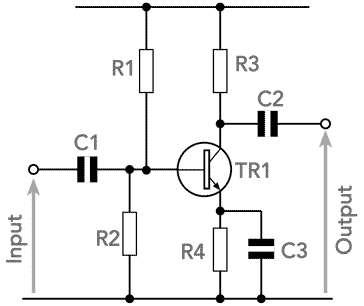
Common emitter transistor amplifier with DC bias & AC coupling
The circuit below shows the electronic circuit design for a common emitter amplifier with resistors to give the required bias for linear operation as well as coupling and decoupling capacitors for AC operation.

Within the circuit there are a number of components that provide different functions to enable the overall circuit to operate in the fashion required:
| R1, R2 | These resistors provide the bias for the base of the transistor. | |
| R3 | This is the collector load resistor within the common emitter amplifier. | |
| R4 | This resistor in the common emitter amplifier provides a measure of DC feedback to ensure that the DC conditions within the circuit are maintained. | |
| C1, C2 | These capacitors provide AC coupling between stages. They need to be chosen to provide negligible reactance at the frequencies of operation. | |
| C3 | This is a bypass capacitor. The effect of R4 is to reduce the gain of the circuit. Bypassing the resistor enables greater levels of AC gain to be achieved. | |
The circuit shown above is that if a basic AC coupled common emitter amplifier.
The common emitter circuit can be used in a variety of forms. - sometimes as a transistor logic output, a directly coupled amplifier and in many areas. It is widely used, providing a good compromise between voltage and current gain along with input and output impedance.
 Written by Ian Poole .
Experienced electronics engineer and author.
Essential bipolar transistor data:-
Make your BJT transistor selection with op-amp data as well as distributor price and availability.
Check it out now!
More Circuits & Circuit Design:
Op Amp basics
Op Amp circuits
Power supply circuits
Transistor design
Transistor Darlington
Transistor circuits
FET circuits
Circuit symbols
Return to Circuit Design menu . . .