How to Design an Op Amp Inverting Amplifier
All you need to know about how to design an operational amplifier, op-amp inverting amplifier circuit with equations, design details, circuit, calculations and design tips.
Op-amp Circuits Include:
Introduction
Circuits summary
Circuit design hints & tips
Inverting amplifier
Summing amplifier
Non-inverting amplifier
Inverting vs non-inverting circuits
Variable gain amplifier
High pass active filter
Low pass active filter
Bandpass filter
Notch filter
Comparator
Schmitt trigger
Multivibrator
Bistable
Integrator
Differentiator
Wien bridge oscillator
Phase shift oscillator
The op amp inverting amplifier circuit is very easy to design and can be implemented with a very limited number of additional electronic components.
In its simplest form the op amp inverting amplifier only requires the use of two additional resistors to be included within the electronic circuit design process. This makes the circuit very simple and easy to implement whilst still providing a very high level of performance.
This the inverting amplifier can also be used as a virtual earth mixer or summing amplifier, but it is also worth noting that the input impedance of this op amp circuit is not as high as the inverting format. As a summing amplifier, this op amp circuit finds many applications within audio mixers as well as many other electronic circuit designs where voltages need to be summed together.
For many people, the op amp inverting amplifier is their favourite form of amplifier circuit with an easy circuit design process, and high levels of performance.
Video: Operational amplifier inverting amplifier circuit
Op amp inverting amplifier circuit
The basic diagram for the inverting operational amplifier circuit is quite straightforward and only needs a few additional electronic components beyond the op-amp chip itself.
Obviously the circuit is based around an operational amplifier, which is a differential amplifier with two inputs: inverting and non-inverting.
The circuit consists of a resistor from the input terminal to the inverting input of the circuit, and another resistor connected from the output to the inverting input of the op-amp. The non inverting input is connected to ground.

In this op amp circuit the feedback is determined by the resistor from the output to the inverting input and the overall resistance from the inverting input to ground, i.e. the input resistor as well as the source resistance of the signal source.
Inverting amplifier gain
One of the main features of the inverting amplifier circuit is the overall gain that it produces. This is quite easy to calculate.
It is simple to determine the gain of this op amp circuit. The voltage gain, Av, is actually the output voltage (Vout) divided by the input voltage (Vin), i.e. it is the number of times the output voltage is larger than the input voltage.
It is also easy to determine the equation for the voltage gain. As the input to the op-amp draws no current this means that the current flowing in the resistors R1 and R2 is the same. Using ohms law Vout /R2 = -Vin/R1. Hence the voltage gain of the circuit Av can be taken as:
Where:
Av = voltage gain
R2 is the feedback resistor value
R1 is the input resistor value
As an example, an amplifier requiring a gain of ten could be built by making R2 47 kΩ and R1 4.7 kΩ as the ratio between the two resistors is ten. Equally the same gain could be obtained using a 33kΩ resistor for R2 and a 3.3kΩ resistor for R1.
Although almost any set of values could be chosen for R1 and R2, the key to the actual selection often rests on other aspects like the input resistance as we will see below, and also in keeping the values for the resistors within reasonable bounds as detailed in the hints and tips section below.
Inverting amplifier input impedance
One consideration in any design like this is the input impedance, because a low impedance might load the previous stage. Often the input impedance should be a factor of ten higher than the output impedance of the previous stage if it is not to load it unduly.
In some instances it might be necessary to have a particular input impedance for microphones that might work better into a specific load.
It is very simple to determine the input impedance of an inverting operational amplifier circuit. It is simply the value of the input resistor R1.

It is easy to reason why the input impedance to the amplifier circuit is equal to R1.
The non-inverting input is connected to ground and therefore this is properly at ground potential.
The gain of the operational amplifier is very high, this means that for outputs within the rail voltage, which it is for an analogue amplifier, the voltage difference between the inverting and non-inverting inputs must be very small. As the non-inverting input is at ground, the inverting input must be virtually at ground. It is for this reason that the circuit is sometimes referred to as a virtual earth amplifier.
Op amp inverting amplifier design hints and tips
The op amp inverting amplifier is very easy to design, but as with any design there are a few hints and tips that can be of use.
- Don’t make R2 too high: Although the input impedance of op amps is high, in any op amp circuit it is always best to ensure that the value of R2 is not chosen to be too high otherwise other circuit effects may load it and the value of gain may not be what is expected. It is often wise to keep the value of R2 below 100kΩ as a rough rule of thumb.
- Don’t make R1 too low: It is also wise not to make the value of R1 too low in this op amp circuit. Remember that it determines the input resistance of the inverting amplifier circuit. If AC coupling the input circuit, the value of the series coupling capacitor will need to be chosen so that its reactance is sufficiently low at the lowest frequencies needed. Lowering the value of R1 increases the value of capacitor required. Also making R1 too low increases the loading on the previous stage.
- Keep the gain down: One of the points to remember when designing with op amps, is not to expect too much gain.Even though the open loop gain can be very high, do not expect that enormous gains can be achieved over the whole of the bandwidth with minimum distortion. Think carefully when the voltage gain goes over, say, about 10 to 20.
- Remember bandwidth: Although op amps have a high value of gain, this starts to fall at increasing frequencies. Even with feedback in the inverting amplifier, the gain bandwidth product needs to be considered. Don’t try to get too much gain out of a single stage op amp circuit, otherwise the frequency response may suffer.
Ensure the output doesn't clip: For most circuits, minimising the distortion is important. One of the circuit design considerations must be to ensure that there is sufficient margin on the output so that the maximum output voltage does not approach the supply rail causing the output to clip.
Often this can happen when large amounts of gain are used, so it is worth making calculations about the maximum output voltage at an early part of the design.
These are only three tips for the circuit design of an op amp inverting amplifier that have been found useful over the years. The main concept is to keep an open mind as to things that might happen in the circuit under unusual circumstances. It also helps not to stretch the circuit design too far, expecting too much from a single stage. Having the tips and these points in mind when designing the circuit can help avoid issues later.
To help your home lab or workshop . . . . . .
To help you with your home workshop or radio shack, etc, we thought these might help:

85PCS 10 Types NE555 LM324 LM393 UA741 ULN2803 LM358 LM386 NE5532 ULN2003 PC817 Integrated Circuit DIP IC Kit
This kit is ideal for home workshops and electronics labs as it provides a good selection of operational amplifiers, op-amps, and other useful integrated circuits.

10PCS UA741CN 741 operational amplifier DIP-8
The 741 is possibly the most famous operational amplifier. Even today, it is a great "jelly bean" chip that is a great general purpose IC, which is widely available and very cheap.

LM358 Surface Mount SOIC-8 Low Power Dual Operational Amplifier choice of 5 or 10 pcs
The LM358 is a well known and used Op-Amp. This version is in a surface mount SOIC-8 package and is available in either 5 or 10 pcs.
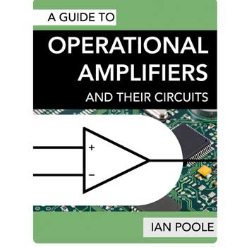
A Guide to Operational Amplifiers and Their Circuits
Written by Ian Poole, this PDF downloadable ebook gives a great introduction to operational amplifiers: what they are, how they work, some circuits with design calculations, hints and tips . . . . in fact all you need to know to get started.
Check out more items you might like from my Components store.
More convenient to buy from Amazon.com? Check out Op-Amps on my Amazon Storefront.
Note: We make a small commission from any sales at no cost to you.
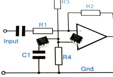
Inverting amplifier single ended operation
Typically an op amp circuit will be operated from differential supplies, e.g. +12V and -12V. This is quite acceptable in many applications, but in many electronic circuit designs only one supply may be available.
Under these circumstances it is relatively easy to implement what is termed a single ended version of the inverting amplifier op amp circuit - this uses only one supply and ground.

The single voltage supply version of the op amp circuit for the inverting amplifier circuit uses more components when compared to the dual rail version, but the design of the amplifier elements remains the same.
Effectively a half way point is created for the non-inverting input. And in this way the operational amplifier sees the same conditions it would as if it were operating from a dual supply.
A few points to note for the electronic circuit design process:
- Half supply point: A point at half the supply voltage is set to connect to the non-inverting input. This is created by the potential divider chain consisting of resistors R3 and R4. In view of the high input impedance of the operational amplifier, values of something like 47kΩ can be used - the current required by the input of the op amp will be small and these values will be good for most op amps . If the values are chosen to be too high then the impedance of the inverting input may offset the voltage.
Decoupling: The half rail supply requires decoupling to ground because the inverting input needs to appear as a signal ground whilst also being maintained at the half supply voltage. The value of the capacitor C1 is chosen so that its impedance is the same as the resistors R3 and R4 in parallel at the lowest frequency required - this gives a -3dB point at this frequency. If a totally flat response is required below this, then a larger capacitor must be used.
By having a relatively high value resistors for R3 and R4, the value of the capacitor does not need to be too high to enable a low value for the low frequency break point to be obtained.
Choice of half rail voltage: The half rail voltage is chosen to be close to 50% of the rail. In this way the circuit will enable the largest output voltage swing up and down without clipping.
Care must be taken to ensure that the overall rail voltage is sufficient for the correct operation of the op amp - consult the data sheet to ensure that the rail value chosen is acceptable for the op amp that has been chosen.
Circuit coupling: A single ended voltage rail op amp inverting amplifier requires the inputs to the AC coupled. Capacitors C2 and C3 should be chosen to pass the lowest signal frequencies with no undue attenuation.
These capacitors should be chosen so that their impedance matches the impedance of the circuit at the lowest frequency required. This makes this point the -3dB point for each of these circuits.
Remember that the input impedance for the circuit could be that of R2, assuming that the circuit is drive by a low impedance source. For the output circuit, the op amp can be assumed to have zero impedance for this calculation, and therefore the resistance or impedance for the output circuit is that of the intended load.
The single ended rail version of the op amp circuit finds applications where only one voltage supply rail is available. Often circuits running from battery supplies will only have one supply and this solution is often employed in these applications.
There are some op amps that are designed to operate in a single ended mode, but this approach can be adopted for op amps that are available.
An operational amplifier is a differential amplifier, and therefore there are two inputs: for the inverting amplifier, the negative feedback from the output and the input signal are both applied to the inverting input, whilst the non-inverting input is taken to ground.
The op amp circuit for the inverting amplifier offers many advantages including relatively low input impedance, a low output impedance and the level of gain that is required (within the limits of the op amp and the gain required from the overall circuit. It also requires very few electronic components to produce a high performance circuit.
 Written by Ian Poole .
Experienced electronics engineer and author.
Essential operational amplifier data:-
Make your op-amp selection with op-amp data as well as distributor price and availability.
Check it out now!
More Circuits & Circuit Design:
Op Amp basics
Op Amp circuits
Power supply circuits
Transistor design
Transistor Darlington
Transistor circuits
FET circuits
Circuit symbols
Return to Circuit Design menu . . .