
PCB Design Layout Guidelines
An overview or tutorial about the basics of PCB design guidleines and the points to watch during PCB design and printed circuit board layout.
PCB Design Includes:
PCB design basics
Schematic capture & drawing
PCB layout / routing
PCB design guidelines
PCB signal integrity
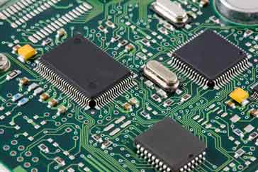
Printed circuit board, PCB design, is one of the most important design elements within the design of an electronics product. In most instances an electronics hardware design engineer will design the circuit, and then a PCB layout specialist will undertake the PCB layout and design from a schematic provided using a PCB CAD system.
The PCB layout and design is a specialist skill requiring knowledge of not only of the PCB design software and PCB CAD system, but also a variety of standards and techniques used to ensure that the basic circuit design is successfully transferred to an overall printed circuit board that can be manufactured in an electronics circuit manufacturing environment.
In order that a printed circuit board can be designed satisfactorily, it often helps to have some guidelines that can be followed, although there is no substitute for experience.
PCB design guidelines
There are many ideas and guidelines that can be drawn up for the design and layout of a PCB. The list below covers a number of them. Obviously there are more, and the PCB design guidelines list below should not be thought of as a complete list.
In order that the PCB design guidelines can be followed more easily, the guidelines are split into sections :
- Board constraint design guidelines - those covering the initial constraints on the board
- Overall layout design guidelines
- Guidelines associated with the planes or layers
- Track design guidelines
- Thermal issues
- Signal integrity and RF considerations
These form some of the main areas for consideration for designing a PCB. For some designs, some of the PCB design guidelines will be more important than others, and judgements will often need to be made to balance one requirement against another.
Board constraint PCB design guidelines
These PCB design guidelines are associated with the constraints of the overall board:- size, shape, and some of the factors that affect the overall design or concept of the PCB. These should be some of the first factors to be addressed.
- Choose reference points that suit the manufacturing process. It is normally necessary to have reference holes or points on the board. These are used for pick and place machines and test fixtures. They should be chosen to suit the PCB manufacturing process. Often they may be holes for fixtures, but they may also be crossed marks for optical sensors. They must be clear of components, and not obscured.
- Allow adequate board area for the circuit Often the dimensions of the board will be defined by the overall product size, but before the PCB design starts, estimates should be made regarding the size of the board and whether it can accommodate the components and their tracks.
- Determine the number of layers required It is wise to determine the number of track layers that are needed within the printed circuit board at the beginning of the design. Additional layers increase the production costs, but may mean that the tracks can be accommodated. Complex designs may have many tracks, and it may not be possible to route them unless sufficient layers are available.
- Consider the board mounting method It is necessary to consider how the printed circuit board will be mounted at the beginning of the design. Different methods of mounting may require different areas of the board to be kept free, or they may take up different areas on the board.
Overall layout PCB design guidelines
These PCB design guidelines should be addressed before the main design of the circuit starts. They should effectively be some of the first elements of the component placement.
- Draw and overview plan of where the different circuit areas will be located One of the first parts of the circuit layout is to draw a rough plan of where the major components and component areas will be located. In this way critical track runs can be assessed along with judging the most convenient design
PCB design guidelines associated with the planes or layers used
It is common practice to use a complete layer or plane for earth or power rails. The most effective ay these can be used must be considered early in the PCB design.
- Consider whether complete planes will be used for power, earth, etc It is common practice to use a complete plane for earth and some major power rails. This has advantages in terms of noise, and current capability.
- Avoid partial planes It is wise to avoid leaving large gaps in earth planes or power planes, or having partial planes in a certain area of the board. These can set up stresses in the board which can lead to warping during manufacture of the bare board, or later when the board is heating during the soldering process. Warping after surface mount components have been added can lead to component fractures and hence a high rate of functional failures.
Track design guidelines
Consideration about the aspects of the tracks on the printed circuit board themselves needs to be given at an early stage as there are trade-offs that may need to be made.
- Determine the standard track width to be used It is necessary to balance the standard track size to be used within the design. If the tracks are too narrow and too close there is a greater possibility of short occurring. Additionally if they are too wide and too far apart then it can restrict the number of tracks in a given area and this may force the use of additional planes in the boards to ensure the PCB design can be routed.
- Consider track size for lines carrying current The thin tracks used in today's printed circuit boards can only carry a limited current. Consideration needs to be given to the size of track for any that carry power rails rather than low level signals. The table below gives some track widths or a 10degree C temperature rise for different thickness copper boards.
| Recommended Maximum Current for PCB tracks |
||
|---|---|---|
| Current (Amps) |
Width for 1 oz board (Thous) |
Width for 2 oz board (Thous) |
| 1 | 10 | 5 |
| 2 | 20 | 15 |
| 3 | 50 | 25 |
- Fix the printed circuit board pad to hole ratio and size At the beginning of the PCB design it will be necessary to determine the pad and hole dimensions. Typically a ratio of about 1.8: 1 (pad : hole) is used, although sometimes a pad 0..5 mm larger than the hole is used as the measure. This allows for hole drilling tolerances, etc. The manufacturer of the bare PCB will be able to advise on the standards that are required for their process. The ratio becomes more important as the size of the pads and holes reduces, and it is particularly important for via holes.
- Determine PCB pad shapes Component libraries associated with PCB CAD systems will have libraries for the schematic and PCB footprints for the different components. However these may vary according to the manufacturing process. Typically they need to be large for wave soldering than for infra-red reflow soldering. Thus the manufacturing process needs to be determined before the design starts so that the optimum pad sizes can be chosen and used on the PCB CAD system and hence on the printed circuit board itself.
Thermal issues
Although for many smaller printed circuit boards thermal issues do not present a problem, with higher processing speeds and higher component densities for modern PCBs, thermal issues can often start to become a significant hurdle.
- Allow sufficient space for cooling around hot components Components that dissipate large amounts of heat may require additional space around them. Allow sufficient space for heatsinks that may be required.
Signal integrity and RF considerations
There are many issues with PCB design associated with Signal integrity, RF and EMC considerations. Many of the ways to avoid problems are associated with the way tracks are routed.
- Avoid running tracks in parallel Tracks that run in parallel for any length will have a higher level of crosstalk with signals on one track appearing on another. Crosstalk can lead to a variety of problems in the circuit and it can be very difficult to eliminate once the printed circuit board has been designed and built.
- When tracks need to cross have them cross at right angles To reduce the level of crosstalk generated, when two signal lines need to cross, they should cross at right angles to reduce the level of capacitance and mutual inductance between the two lines.
There are a host of PCB design guidelines that can be documented. The PCB design guidelines here are just a few of the many that could be devised, but they can form the basis of a set of guidelines that could be used general PCB design.
 Written by Ian Poole .
Experienced electronics engineer and author.
More Circuits & Circuit Design:
Op Amp basics
Op Amp circuits
Power supply circuits
Transistor design
Transistor Darlington
Transistor circuits
FET circuits
Circuit symbols
Return to Circuit Design menu . . .


