How to Design a PCB: printed circuit board layout
When designing printed circuit baords, there are several key stages you need to know how to undertake to produce the best PCB design for a given application.
PCB Design Includes:
PCB design basics
Schematic capture & drawing
PCB layout / routing
PCB design guidelines
PCB signal integrity
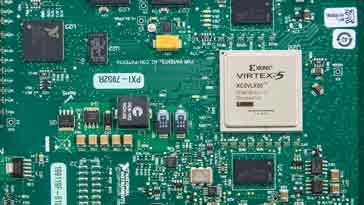
Knowing how to design a printed circuit board, PCB is a key element of any electronic circuit design process.
The PCB layout and design has a major impact on the way in which a circuit work, and therefore if the printed circuit board is designed in an effective way, then the circuit will perform more reliably and within its specification.
PCB design equipment
For commercial development programmes there are may CAD, computer aided design packages available that are needed as a result of the complexity.
Even for the student and hobbyist there are many very good packages that are either free of can be obtained for a modest cost.
The old PCB design process of using tape placed on a master drawing sheet are long gone, although it is possible this may still be done in a number of very limited cases.
The PCB software capability varies considerably. Budget, or even free software provides the basic functions, whereas the top end packages enable many more facilities to be incorporated into the design. Simulations, complex routing, and many more facilities are available.
The ability to undertake simulations is becoming an increasing requirement with the speeds of digital boards increasing, and radio frequency designs reaching ever higher frequencies.
Circuit schematic capture
The first stage in the development of a PCB design is to capture the schematic for the circuit. This may be achieved in a variety of ways. Circuits may be entered into a schematic capture tool. This may form part of the PCB design suite, or it may be an external package whose output can be exported in a suitable format.
In addition to purely performing the schematic capture, simulations of the circuit may be undertaken at this stage. Some packages may be able to interface to simulation packages. For applications such as RF circuit design simulation of the circuit will enable the final circuit to be optimised more without building a prototype.
With the schematic capture complete the electronic design of the circuit is contained within the file and can be converted to what is termed a "netlist". The netlist is the interconnectivity information and it essentially the component pins and the circuit nodes, or nets, to which each pin connects.
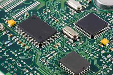
Initial PCB component placement
Before proceeding with the detailed PCB design and layout, it is necessary to gain a rough idea of where components will be located and whether there is sufficient space on the board to contain all the required circuitry. This will enable decisions about the number of layers needed in the board, and also whether there is sufficient space to contain all the circuitry may need to be made.
Once a rough estimate has been made of the space and approximate locations of the components, a more detailed component layout can be made for the PCB design. This can take into account aspects such as the proximity of devices that may need to communicate with each other, and other information pertaining to any RF considerations for example.
In order that components can be incorporated into the PCB design they must have all the relevant information associated with them. This will include the footprint for the printed circuit board pads, any drilling information, keep out areas and the like. Typically several devices may share the same footprint, so this information does not have to be entered for each component part number. However a library for all the devices used will be built up within the PCB layout design system. In this way components that have been used previously can be called up easily.
Routing
Once the basic placement has been completed, the next stage of the PCB design is to route the connections between all the components. The PCB software then routes the physical connections on the board according to the netlist from the schematic. To achieve this it will use the number of layers that are available for connections, creating via holes as required. Often one layer will be allocated for use as a ground plane, and another as a power plane. Not only does this reduce the level of noise, but it enables low source resistance connections to be made for the power.
The routing can use a significant amount of computing power. This is particularly true for larger designs where there may be upwards of three or four thousand components. Where routing is difficult as a result of high component density, this can result in the routing taking a significant amount of time.
PCB files: Gerber files, etc
The information for the photo plots of the PCB layout are outputted in the form of Gerber files. This format is the standard for PCB files and they are a form of numerical control file that is used by a photo plotter. In addition to the Gerber files, drill information is also generated along with the screen print and photo-resist information.
One major element in the cost of a printed circuit board is the drilling. In any design some holes are required for fixing as well as those required for any conventional components needed. However to reduce costs it is wise to use as few hole sizes as possible. In this way the drill will need changing less and time can be reduced.
Once complete the information for the PCB will be used in many areas of the manufacturing process. Not only will it be used for the manufacture of the actual PCB itself, but the files will also be used in other areas of the manufacturing process. They may be used to develop a pick and place programme, and in addition to this the files may be used in the manufacture of a PCB solder mask for adding solder paste to the board prior to component placement. The files may also be used for developing various forms of test programme such as an "In-Circuit Test" (ICT), and particularly in developing any bed of nails test fixture. In this way, the PCB design is a crucial element of the whole manufacturing process for any product. The PCB design is more than just a design for the basic board.
 Written by Ian Poole .
Experienced electronics engineer and author.
More Circuits & Circuit Design:
Op Amp basics
Op Amp circuits
Power supply circuits
Transistor design
Transistor Darlington
Transistor circuits
FET circuits
Circuit symbols
Return to Circuit Design menu . . .