LM317 Voltage Regulator Circuits
The LM317 voltage regulator IC is a well established chip that can be used in a variety of circuits with just a few additional electronic components to make an effective fixed or adjustable voltage regulator.
Linear Power Supply Circuits Primer & Tutorial Includes:
Linear power supply
Shunt regulator
Series regulator
Current limiter
Constant current vs foldback limiting
78** series regulators & circuits
LM317 voltage regulator & circuits
LDO, low dropout regulators
See also:
Power supply electronics overview
Switch mode power supply
Capacitor smoothing
Over-voltage protection
PSU specs
Digital Power
Power management bus: PMbus
Uninterruptible power supply
The LM317 is an established and popular integrated circuit that provides a highly effective linear voltage regulation capability in one integrated circuit.
The LM317 is a three terminal device that enables a positive linear voltage regulator circuit to be very easily designed that is capable of providing 1.5 amps over an output voltage range of 1.2 to 37 volts, dependent upon the input voltage obviously.
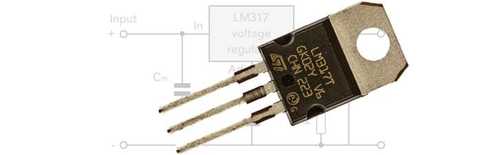
The integrated circuit requires just a few external electronic components to complete the electronic circuit design which can be used in a very large variety of applications.
These applications can include separate linear voltage regulation in a power supply, local voltage regulation, on-card voltage regulation, and it can even be made into a programmable voltage supply with a few additional electronic components.
Also be changing the circuit slightly, the LM317 voltage regulator integrated circuit can be used as a precision current regulator or current limiter for a power supply.
LM317 basic specification
The LM317 voltage regulator integrated circuit offers a really excellent level of performance as seen by the summary specification given below.
| Summary Specification for the LM317 Voltage Regulator |
||||
|---|---|---|---|---|
| Parameter & conditions | Min | Typical | Max | Units |
| Max Current (TO220 on heatsink) | 1.5 | 2.2 | A | |
| Output voltage (range set by design) | 1.2 | 37 | V | |
| Line Regulation 3.0 V≤ VI−VO ≤ 40 V | 0.01 | 0.04 | %/V | |
| Load Regulation 10 mA ≤ IO ≤ Imax Vo ≤ 5V | 5 | 25 | mV | |
| Load Regulation 10 mA ≤ IO ≤ Imax Vo ≥ 5V | 0.1 | 0.5 | %/Vo | |
| Adjustment pin current !,sub>Adj | 50 | 100 | µA | |
| Reference voltage (nominal) (Vref) | 1.2 | 1.25 | 1.3 | V |
| Line Regulation 3.0 V ≤ VI−VO ≤ 40 V | 0.02 | 0.07 | &/V | |
| Load Regulation 10 mA ≤ IO ≤ Imax with Vo ≤ 5.0V | 20 | 70 | mV | |
| Load Regulation 10 mA ≤ IO ≤ Imax with Vo ≥ 5.0V | 0.3 | 1.5 | %/Vo | |
| Temperature Stability (Tlow ≤ TJ ≤ Thigh) | 0.7 | % Vo | ||
| Minimum Load Current to Maintain Regulation | 3.5 | 10 | mA | |
Note: It should be noted that there are a number of different variants of the LM317 and the chip is made by a number of different manufacturers. This means that there are several variants with different specifications. Those given in details above are typical and generally used. However for exact details the data sheet for the particular manufacturer should be consulted.
The LM317 has been available for many years and is an established electronic component. Although it has been available for many years, it offers a level of performance which is more than sufficient for most electronic circuit designs, offering good regulation, low component count, low noise output and a variety of other specifications.
The fact that the chip has been available for many years means that it is manufactured by a number of companies and as a result it is unlikely to go obsolete, and this is a distinct advantage for anyone considering starting a new design.
LM317 pinouts & packages
The LM317 regulator IC is available in a number of packages, both for standard leaded configurations and also as a surface mount device, SMD. The choice of the type of format will obviously depend upon the particular electronic circuit design and how it will be manufactured.
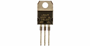
For electronic circuit designs where the construction will use a leaded form of construction, the TO220 style is the most popular. It is necessary to be aware that the LM317 pinout connections are not the same as for the popular 78xx series ICs where the centre pin is the common and the input and output are either side.
Also be aware that the heatsink metal contact is connected to the output, so it will be necessary to use an insulator kit to bolt it to the heatsink should one be needed.

For surface mount construction, the surface mount device version uses the D2PAK package. Gain the Input and Adjust pins are on outer most positions, and the small centre stub is the output - this is also connected to the metal contact for the heatsink. Being on a PCB this will not need an insulating washer as the PCB copper will be able to be used as a contact, and also for conducting heat away.

Ideas for your projects . . . . . .
This great value equipment has been selected for your interest and it is available via AliExpress. Alternatively check out my Amazon .com Storefront.

Linear Voltage Regulators Kit: LM317, 7805, 7812, etc
This kit contains a total of 50 TO220 package voltage regulator ICs which include: LM317T L7805CV L7806CV L7808CV L7809CV L7810CV L7812CV L7815CV L7818CV L7824CV

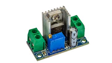
LM317 Adjustable Regulator Kit
Based around the reliable LM317 regulator chip, this kit contains all the components to make a continuously adjustable DC regulator 1.5V - 12V - ideal for teaching & training. Requires a DC smoothed input.

0-30V 2mA-3A DC Regulator Kit
This regulator provides a great way of creating a variable output voltage from a DC smoothed supply. For higher current levels it will require an additional heatsink for the pass device, otherwise it receives good reviews.
. More Linear Regulators . . .
More convenient to buy from Amazon.com?
Note: We make a small commission from any sales at no cost to you.
Operation of the LM317
The LM317 voltage regulator chip is almost completely self contained, requiring just a few external electronic components to complete the circuit.
This voltage regulator chip is a three terminal floating regulator - it develops a nominal 1.25 volts internal reference voltage referred to as Vref between the output and adjustment terminals.
This reference voltage is then converted to what is termed a programming current, IPROG by the resistor R1, and then a constant current flows through the resistor R2 to ground.

It is because of the 1.25 volts reference voltage between the Adjustment terminal, Adj and the output that the minimum output voltage attainable is 1.25 volts.
The regulated output voltage is given by the equation below and this means the output voltage or voltage range can be set by selection of the resistor, using a variable resistor if a variable output is needed.
Note:
1) Since IAdj is controlled to less than 100 mA, the error associated with this term is negligible in most applications and it is normally ignored. It may be required for some specialist exacting circuit designs.
2) Vref is equal to approximately 1.25 volts - see specification.
It is worth noting that as a result of the fact that the LM317 is a floating voltage regulator, and it is only the voltage differential across the circuit which is important to performance, it is possible for it to operate at high voltages with respect to ground is possible, although it won't be able to give regulation and control over the full range of the high voltage.
External capacitors to improve circuit performance
Although it is possible to get the LM317 voltage regulator to work with just two additional electronic components - both resistors to set the voltage, some capacitors may be used to help improve the performance.
It is recommended that a 0.1µF ceramic capacitor, or a 1 µF tantalum capacitor is placed across the input - C>in. The use of this will overcome any sensitivity to to the input line impedance. Sometimes a long line from any smoothing capacitor, etc might lead to some instability int he circuit. The use of Cin will overcome this issue.
The adjustment terminal can be bypassed to ground as this will improve ripple rejection. The capacitor, CAdj prevents ripple from being amplified, particularly as the output voltage is increased.

Normally a capacitor of around 10µF should give an improvement in ripple rejection of about 15 dB at 120 Hz in a circuit with a 10 V output.
It helps to have a capacitor on the output, C>out to improve the transient response. However certain values of capacitor can lead to excessive ringing. Capacitors of around 1.0 µF tantalum or 25 µF aluminium electrolytic capacitor on the output swamps this effect and ensures the voltage regulator circuit remains stabile.
LM 317 circuit with external protection diodes
When there is capacitance present in a circuit driven by a voltage regulator such as an LM317, either directly on the output of the regulator or within the circuit being driven, it is often wise to add protection diodes to prevent the capacitors from discharging through low current points into the regulator.

Protection diodes are recommended for output voltages in excess of 25 V or when high values of capacitance appear on the output of the regulator. It is often recommended that for capacitance values in excess 25 µF and when the values for CAdj exceed 10 µF).
In the circuit the diode D1 prevents the overall capacitance on the output from discharging through the IC during an input short circuit. The output capacitance consists of COut plus any capacitance in the circuit being powered. Although an input short circuit may appear unlikely, the path through any input circuitry may appear as a short circuit under some conditions.
Also the diode D2 protects against the capacitor CAdjj discharging through the IC during an output short circuit.
Finally, the combination of both diodes prevent CAdj from discharging through the IC during an input short circuit.
The diodes, D1 and D2 need not be any special form of diode - diodes such as the 1N4002 have sufficient current capability and reverse breakdown capability to provide excellent protection. 1N4002s are also very cheap and widely available.
0 - 30 V LM317 regulator circuit
The basic LM317 voltage regulator circuit provides for voltage adjustment between about 1.25 and 30 volts. For many applications a variable supply of zero to 30 volts would be better.
By adding a few additional electronic components, the LM317 can be made to provide a continuously variable voltage regulated supply covering 0 - 30 volts.

The calculations for this voltage regulator circuit is very straightforward:
Although suggested values have been incorporated within the circuit diagram, it is possible to alter these as well as adding additional capacitors to provide the exact electronic circuit design and performance needed.
LM317 current limiter circuit
The LM317 can be used to provide a current limiter function. The circuit is very straightforward and as the chip does not require referencing to ground, this circuit can simply be placed in line.

The calculations for the LM317 current limiter are very straightforward:
It should be remembered that Vref is nominally 1.2 or even 1.25 volts, and it should also be remembered that the resistor should have sufficient heat dissipation capacity to carry the current being required of it.
Issues with variable regulator circuit: options for failsafe circuit
The LM317 is easily used as a variable regulator, and the variable resistor used can even be used as a print panel control on a variable voltage power supply.
One of the issues with potentiometers is that after persistent use, or when used in a dirty environment the track can become contaminated, and the slider will become open circuit as it passes over the track.
As can be seen from the circuit examples above, the circuits are very straightforward. However in many instances only two ends of the potentiometer may be used: the slider and one end of the fixed resistor.

While this is not good circuit design practice, this often happens for a variety of reasons.
If the track becomes dirty, then the slider can become intermittent and the resistor will become open circuit, if only for short periods of time. When this happens it can be seen fromt he equation determining the output voltage that the output voltage will rise significantly, and could damage any circuits being powered.
One solution is to make sure that the end of the potentiometer is connected and then any voltage rise will be limited to that determined by the ratio of R1 and R2.
AN even more elegant solution involves the use of a single transistor and rather than the output voltage rising, it will fall, thereby eliminating and issues of overvoltage damage.

The circuit shows an LM317 with an additional transistor. Should the slider contact on the potentiometer fail and become open circuit, then the transistor TR1 will turn on and the ADJ terminal on the LM317 will be pulled down to around 1V thereby averting the disaster of putting an overvoltage on the output.
Find out Voltage Regulator Data:
Check out the data for a large variety of voltage regulators along with the distributor stock levels and prices.
Find out more about Voltage Regulator Chips & Data
LM317 circuit design tips
In order to ensure the best performance from any LM317 voltage regulator circuit, there are a few electronic circuit design tips that can help ensure that the circuit will have the best chance of performing well.
Ensure wiring & PCB conductors etc large enough: It must be remembered that the LM317 voltage regulator can handle current levels of up to 1.5 amps or a little more under some circumstances. To keep any voltage drops as low as possible, the wiring must be sufficient to handle the current. Remember, voltage drops in the output wiring can degrade the regulation performance as voltage drops here will vary with current taken.
Keep programming resistor close to regulator: For best performance, the programming resistor, R1 should be connected as close to the regulator as possible. This minimises any voltage drops which appear on top of the voltage developed by the reference and this degrades the regulation of the circuit.
Keep ground end of R2 close to load ground: The ground end of R2 should be connected close to the load connection. This provides a form of remote ground sensing and improves the overall load regulation.
Input decoupling capacitor placement: It is important to place the input capacitor, Cin as close to the input terminal as reasonably possible and a short length of conductor to the system ground.
Minimise loop area for Cin connection: In order to ensure the minimum pickup and stray induction, etc, keep the loop area formed by the bypass capacitor connection, the input terminal, and the system GND as small as possible.
Consider additional HF decoupling for Cin: As some tantalum and electrolytic capacitors have poor high frequency or HF response, it is worth considering using an additional ceramic capacitor in parallel with the main input capacitor Cin. Typical value might be 0.1µF and this will ensure that any HF noise and responses are suppressed.
These and other general electronic circuit design precautions will help ensure that the LM317 voltage regulator circuit operates so that it provides the very best performance that it can offer.
The LM317 is an excellent voltage regulator chip, which although it has been available for many years, provides excellent performance for a comparatively low cost. The regulator can be obtained quite cheaply and very few other electronic components are needed to make a first class voltage regulator circuit.
In addition to this, the LM317 voltage regulator chip can be utilised to provide several other power supply related functions, thereby making this a very versatile and valuable asset for any electronic circuit design engineer.
 Written by Ian Poole .
Experienced electronics engineer and author.
More Circuits & Circuit Design:
Op Amp basics
Op Amp circuits
Power supply circuits
Transistor design
Transistor Darlington
Transistor circuits
FET circuits
Circuit symbols
Return to Circuit Design menu . . .