Step Up Boost Regulator or Converter
- summary or tutorial about the circuit and operation of a step up or boost regulator using switch mode power supply techniques.
SMPS Power Supply Circuits Primer & Tutorial Includes:
Switch mode power supply
How does SMPS work
Step down buck converter
Step up boost converter
Buck Boost converter
See also:
Power supply electronics overview
Linear power supply
Capacitor smoothing
Over-voltage protection
PSU specs
Digital Power
Power management bus: PMbus
Uninterruptible power supply
One of the advantages of switch mode power supply technology is that it can be used to create a step up or boost converter / regulator.
Boost converters or regulators are used in many instances from providing small supplies where higher voltages may be needed to much higher power requirements.
Often there are requirements for voltages higher than those provided by the available power supply - voltages for RF power amplifiers within mobile phones is just one example.
Step-up boost converter basics
The boost converter circuit has many similarities to the buck converter. However the circuit topology for the boost converter is slightly different. The fundamental circuit for a boost converter or step up converter consists of an inductor, diode, capacitor, switch and error amplifier with switch control circuitry.
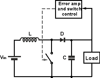
The circuit for the step-up boost converter operates by varying the amount of time in which inductor receives energy from the source.
In the basic block diagram the operation of the boost converter can be seen that the output voltage appearing across the load is sensed by the sense / error amplifier and an error voltage is generated that controls the switch.
Typically the boost converter switch is controlled by a pulse width modulator, the switch remaining on of longer as more current is drawn by the load and the voltage tends to drop and often there is a fixed frequency oscillator to drive the switching.
Boost converter operation
The operation of the boost converter is relatively straightforward.
When the switch is in the ON position, the inductor output is connected to ground and the voltage Vin is placed across it. The inductor current increases at a rate equal to Vin/L.
When the switch is placed in the OFF position, the voltage across the inductor changes and is equal to Vout-Vin. Current that was flowing in the inductor decays at a rate equal to (Vout-Vin)/L.
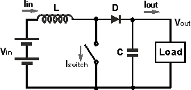
Referring to the boost converter circuit diagram, the current waveforms for the different areas of the circuit can be seen as below.
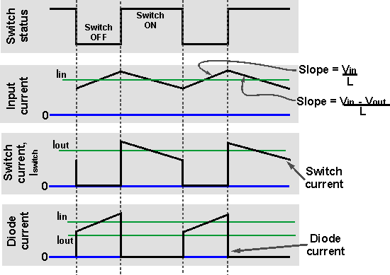
It can be seen from the waveform diagrams that the input current to the boost converter is higher than the output current. Assuming a perfectly efficient, i.e. lossless, boost converter, the power out must equal the power in, i.e. Vin ⋅ Iin = Vout ⋅ Iout. From this it can be seen if the output voltage is higher than the input voltage, then the input current must be higher than the output current.
In reality no boost converter will be lossless, but efficiency levels of around 85% and more are achievable in most supplies.
 Written by Ian Poole .
Experienced electronics engineer and author.
More Circuits & Circuit Design:
Op Amp basics
Op Amp circuits
Power supply circuits
Transistor design
Transistor Darlington
Transistor circuits
FET circuits
Circuit symbols
Return to Circuit Design menu . . .