NPN-PNP Two-Transistor Amplifier Circuit
There are many differnet transistor amplifier configuration - one here uses a PNP and NPN transistor and has the gain defined by two resistors.
Transistor Circuit Collection Include:
Transistor circuit collection
Common emitter
Emitter follower
Common base
Darlington pair
Sziklai pair
Current mirror
Long tailed pair
Constant current source
Capacitance multiplier
Two transistor amplifier
High pass filter
Switch circuits
Pulse generator
Schmitt trigger
One transistor relaxation oscillator
Transistor crystal-oscillator
How to run transistors in parallel
See also:
Transistor circuit design
While a single-stage Class A common-emitter transistor amplifier is a staple of analogue circuit design, it often suffers from limitations regarding gain stability, temperature dependence, and output impedance.
To overcome these drawbacks, designers frequently employ multi-transistor configurations. One particularly elegant and effective solution is the NPN-PNP two-transistor amplifier circuit.
This straightforward electronic circuit design is two transistor amplifier with feedback to offer a defined gain level that can be determined by the resistors in the circuit.
The design includes PNP and NPN transistors and adopts a very similar topology to that of the Sziklai pair, but with additional resistors included to define the gain.
By combining complementary bipolar junction transistors—specifically an NPN device (TR1) for primary voltage amplification and a PNP device (TR2) for output buffering and feedback control—this circuit achieves superior performance, predictable gain, and enhanced DC stability compared to its single-stage counterpart.
Circuit Description and Operation
The accompanying circuit schematic illustrates the typical architecture of an NPN-PNP two-stage amplifier:
- TR1 (NPN Transistor): Acts as the primary active amplifying device. The incoming AC signal is coupled to its base via input capacitor C1, with DC biasing established by resistor network R1 and the lower divider leg.
- TR2 (PNP Transistor): Configured in conjunction with TR1, TR2 handles the output stage and completes the local feedback loop. Its base is driven by the collector voltage of TR1 (dropping across load resistor R3).
- R4 and R5 (Feedback Network): Resistor R4 connects the output node back to the emitter of TR1, while R5 provides the emitter DC path to ground. This local series-shunt (or emitter-current) feedback network is crucial for defining the operating characteristics of the entire amplifier.
- C2: The output coupling capacitor, which blocks DC bias voltages from reaching the subsequent stage while allowing the amplified AC signal to pass through.
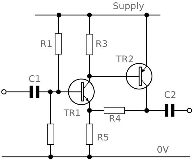
In operation, the input signal modulates the base current of TR1. TR1 amplifies this signal, and its collector voltage drives the base of the complementary PNP transistor TR2. The resulting signal is delivered to the output through coupling capacitor C2, while a portion of the output signal is fed back via R4 to the emitter of TR1.
Voltage Gain and Feedback Control
In a traditional single-stage common-emitter amplifier, the voltage gain is heavily dependent on the internal parameters of the transistor, particularly its current gain ($\beta$ or $h_{FE}$), as well as operating temperature and collector current. Because transistor parameters vary widely from device to device, predicting and stabilizing the exact gain in mass production can be challenging without negative feedback.
In the NPN-PNP two-transistor circuit, the inclusion of the local feedback resistors R4 and R5 brings the voltage gain ($A_v$) under precise external control. The AC voltage gain is primarily determined by the ratio of these external resistors rather than the active device characteristics:
This formula demonstrates that the overall amplification is dictated by passive, high-tolerance components rather than the fluctuating semiconductor properties of TR1 and TR2.
Advantages Over a Traditional Single-Stage Common-Emitter Amplifier
Compared to a standard Class A common-emitter single transistor amplifier stage, the NPN-PNP configuration offers several distinct engineering advantages:
- Precise Gain Stability: Because the gain is set by the external feedback resistor ratio (R4 and R5 ), variations in transistor Β due to component tolerances, aging, or manufacturing spread have minimal impact on overall circuit performance.
- Superior DC Thermal Stability: The direct-coupled feedback loop tightly anchors the DC operating point. This prevents thermal runaway and stabilizes collector currents across a wide operating temperature range.
- Lower Output Impedance: The complementary output arrangement provides a lower output impedance than a typical unbuffered common-emitter stage. This allows the circuit to drive subsequent load stages more effectively without suffering from excessive signal attenuation or voltage sag.
- Improved Linearity and Reduced Distortion: Negative feedback inherently linearises the transfer characteristic of the amplifier. Consequently, the circuit exhibits lower harmonic distortion for moderate signal swings compared to an open-loop single transistor stage.
Stability and Spurious Oscillations
Although this two-transistor NPN–PNP amplifier offers high open-loop gain and well-defined closed-loop biasing through its feedback network, it is susceptible to high-frequency instability and spurious oscillation if left uncompensated. Because the circuit places two inverting common-emitter gain stages inside a single overall feedback loop, its dynamic behaviour shares much in common with an uncompensated operational amplifier.
Each transistor stage introduces pole frequencies determined by its output impedance, bias resistors, and transistor capacitances, including Miller-multiplied collector–base capacitance. As frequency rises, the two stages and the feedback path can accumulate sufficient phase shift that, if loop gain remains greater than unity when phase shift approaches 180 degrees, negative feedback turns into positive feedback and sustains oscillation.
• Common Causes of Instability
- Loop phase shift: Cascading two common-emitter stages creates multiple poles, reducing phase margin at higher frequencies unless the open-loop response rolls off early enough.
- Parasitic VHF oscillations: Lead and track inductance combined with device capacitances and high-$f_T$ transistors can allow VHF oscillation (typically tens to hundreds of megahertz) even when low-frequency feedback appears well behaved.
- Power supply coupling: Shared supply impedance allows signal currents from the output stage to modulate the supply rail and feed back into earlier bias or collector nodes if decoupling is inadequate.
- Capacitive loading: Connecting a capacitive load such as coaxial cable or a following stage with significant input capacitance can introduce an extra pole that erodes phase margin.
• Practical Stabilisation Measures
- Dominant-pole or Miller compensation: Adding a small compensation capacitor (often tens of picofarads, determined by experiment and simulation) across a suitable high-impedance node helps roll off gain before excessive phase shift develops.
- Feedback lead compensation: A small capacitor placed across the feedback resistor can introduce a phase-leading zero to counter stray capacitance at the feedback summing node.
- Base stopper resistors: A low-value resistor (typically a few tens of ohms) close to a transistor base helps damp VHF parasitic resonances without significantly affecting normal signal operation.
- Local decoupling and layout: Keep high-frequency current loops compact, place decoupling capacitors close to the supply rail and ground return, and avoid long, unshielded leads on sensitive nodes.
Summary
The NPN-PNP two-transistor amplifier circuit represents a significant step up in sophistication from basic single-transistor building blocks. By ingeniously combining complementary semiconductor devices with a local feedback network, it successfully trades open-loop gain for exceptional stability, predictability, and linearity—making it a valuable topology in classic analogue design.
This two transistor amplifier is a useful design to have in the electronics engineers toolbox. It is a simple circuit, yet operates effectively in scenarios where a little mroe gain is required than that which could be provided by a single transistor.
 Written by Ian Poole .
Experienced electronics engineer and author.
Essential bipolar transistor data:-
Make your BJT transistor selection with op-amp data as well as distributor price and availability.
Check it out now!
More Circuits & Circuit Design:
Op Amp basics
Op Amp circuits
Power supply circuits
Transistor design
Transistor Darlington
Transistor circuits
FET circuits
Circuit symbols
Return to Circuit Design menu . . .