Transistor Crystal Oscillator Circuit
Transistor crystal oscillators can work very well, but a careful choice of the circuit values is needed in the circuit to provide reliable operation for the circuit design.
Transistor Circuit Collection Include:
Transistor circuit collection
Common emitter
Emitter follower
Common base
Darlington pair
Sziklai pair
Current mirror
Long tailed pair
Constant current source
Capacitance multiplier
Two transistor amplifier
High pass filter
Switch circuits
Pulse generator
Schmitt trigger
One transistor relaxation oscillator
Transistor crystal-oscillator
How to run transistors in parallel
See also:
Transistor circuit design
Crystal oscillators are used in many areas of electronics. Using a crystal oscillator circuit enables a high performance high stability oscillator to be built very cheaply and easily.
Crystal oscillators can be used in a large number of applications in electronics and radio. In some instances crystal oscillators may be used to provide a cheap clock signal for use in a digital or logic circuit.
In other instances a crystal oscillator may used to provide a stable and accurate RF signal source. As a result crystal oscillators are often used by radio hams or radio amateurs in radio transmitter circuits, where they can be particularly effective.
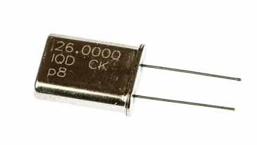
What is a crystal
As the name implies they are made from quartz, a naturally occurring form of silicon, although most of that used for electronics applications is manufactured synthetically these days. The components rely on the remarkable properties of quartz for their operation. When placed into an electronic circuit a crystal acts as a very high quality tuned circuit. In addition to this they are very stable and their resonant frequency does not vary much with time or temperature.
A crystal depends on the piezo-electric effect to work. This effect converts a mechanical stress in a crystal to a voltage and vice versa. In this way the piezo-electric effect converts the electrical impulses to mechanical stress which is subject to the very high Q mechanical resonances of the crystal, and this is in turn linked back into the electrical circuit.
Although not a component that may be bought from any electronics stockist, they can be bought from radio frequency component stockists, or directly from the manufacturer. Outlets are available in most countries.
Note on Quartz crystal resonators:
Quartz crystals have become an essential part of today's electronics providing a high performance resonator at low cost. These components are used as the resonant element in many electronic designs from microprocessor clock oscillators to RF designs for oscillators to high performance stable oscillators and also within crystal filters.
Read more about Quartz crystal resonator technology.
Colpitts crystal oscillator
There is a great number of different types of circuit that can be used for crystal oscillators, each one having its own advantages and disadvantages. One of the most common circuits used for crystal oscillators is the Colpitts configuration as shown below.
The circuit uses a capacitor divider network comprising C1 and C2 to provide the feedback and the output is taken either from the emitter as shown. Alternatively it is possible to place a resistor or choke in the collector circuit and take the output from there. In either case it is wise to employ a buffer after the crystal oscillator circuit to ensure the minimum load is applied.
In this configuration, the crystal operates in a parallel mode. When running in this mode, the crystal should be presented with a load capacitance to operate on its correct frequency. This load capacitance is specified with the crystal and is typically 20 or 30 pF. The crystal oscillator circuit will be designed to present this capacitance to the crystal. Most of this will be made up by the two capacitors C1 and C2, although the remaining elements of the circuit will provide some capacitance.
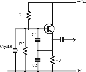
The disadvantage with this circuit is that the resistor bias chain shunts the series combination of C1 and C2 as well as the crystal. This means that additional gain and current are required in the crystal oscillator circuit to overcome this, and also the stability may be affected to some degree. The other effect the bias resistors have is to reduce the Q of the crystal. The problem can be overcome to some degree by using a field effect transistor for the active device, but these devices are generally not as stable as bipolar devices and they often need a higher operating current.
It is also very common for a small trimmer capacitor to be placed across the crystal. In this way the frequency of the crystal oscillator can be finely trimmed to the exact frequency required.
Crystal oscillator component value optimisation
The circuit conditions are fundamentally governed by capacitors C1, and C2 along with the bias resistors R1 and R2, and the emitter resistor R3. As the circuit is frequency dependent the values will change according to the frequency of operation. Typical values are given below.
| Circuit Values for Transistor Crystal Oscillator Circuit Design |
|||||
|---|---|---|---|---|---|
| Frequency range MHz |
C1 pF |
C2 pF |
R1 kohms |
R2 kohms |
R3 kohms |
| 1 - 3 | 330 | 220 | 33 | 33 | 6.8 |
| 3 - 6 | 220 | 150 | 33 | 33 | 6.8 |
| 6 - 10 | 220 | 150 | 33 | 33 | 4.7 |
| 10 - 20 | 150 | 100 | 33 | 33 | 2.2 |
These values will give provide a good solution for many circumstances. The transistor can be a BC109 or similar general purpose transistor.
Crystal oscillator gain and drive level
In order to obtain the best performance from a crystal oscillator, it is necessary to ensure the crystal is driven at the correct level. If the drive level for the crystal is too high then the parasitic resonances of the crystal may be excited. Alternatively the crystal oscillator may even run on the incorrect frequency. Additionally if the drive level is too high then the phase noise performance of the crystal oscillator will be degradedAdditionally the crystal can be damaged if the drive level is too high. In particular the miniature types are susceptible to damage. Even if permanent damage is not caused, the high level of drive within the crystal oscillator increases the rate of ageing and can cause a frequency shift. It is therefore important to ensure the level of drive within the crystal oscillator circuit is approximately correct.
In view of the need to ensure the correct operating conditions for the crystal oscillator itself, it is necessary to optimise the circuit for stability, gain and drive level. This may lead to a lower output level, but this can be overcome in the following stages.
The transistor crystal oscillator circuit described provides a good stable reference signal that will be satisfactory for many applications. In some circumstances highly stable oscillators will be needed and it may be necessary to use a purpose designed and made oven controlled crystal oscillator (OCXO). These are considerably more expensive, but offer very high levels of performance in terms of stability, frequency accuracy and phase noise. If these are needed then the additional cost may be justified.
 Written by Ian Poole .
Experienced electronics engineer and author.
More Circuits & Circuit Design:
Op Amp basics
Op Amp circuits
Power supply circuits
Transistor design
Transistor Darlington
Transistor circuits
FET circuits
Circuit symbols
Return to Circuit Design menu . . .