FRAM Ferroelectric RAM Technology & Operation
Ferroelectric RAM memory technology uses crystals where the dielectric has a reversible electric polarisation.
FRAM Memory Tutorial Includes:
What is FRAM memory
FRAM operation & technology
Memory types:
Memory types & technologies
DRAM
EEPROM
Flash
FRAM
MRAM
Phase change memory
SDRAM
SRAM
Ferroelectric RAM operation and technology is based upon the properties crystals of a dielectric that have a reversible electric polarisation.
FRAM memory technology is non-volatile and it combines this with an almost unlimited number of read-write cycles. FRAM memory technology also offers a very low level of power consumption, making it a contender for the memory for many applications.
Although the technology is less dense than other more established technologies, and has a higher cost, these issues are being addressed as development progresses.
What is the ferroelectric effect
As the name of the memory implies, the ferroelectric RAM technology depends upon the ferroelectric effect for its operation. This effect has the ability for the dielectric used to change its polarisation dependent upon the voltage applied.
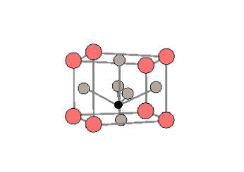
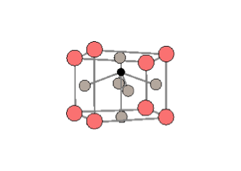
The ferroelectric effecty is observed in a group of materials known as Perovskites. These materials have a crystalline structure with an atom at the centre. This atom has two equal and stable low energy states and these determine the position of the atom.
This is a variety of different compounds that fall into this category. These include substances including: Lead Zirconate Titanate, etc..
If a field is applied to the crystal in the required plane, then the atom will move in the direction of the field. It is the position of the atom that then acts as the determination of the state of the material and in turn this can be used to store data.
The two states of the ferroelectric material are referred to as 'up polarisation' when the atom is on the top position, and 'down polarisation' when the atom is in the bottom position.
Energy required within the transitions, and this means there is a hysteresis loop over which the ferroelectric material operates.

It should be noted that the ferroelectric crystals do not contain any ferrous material. Also they are not affected by magnetism. Instead the materials gain their name from the similarity of the graph of charge plotted as a function of voltage to the familiar BH curve of a magnetic material.
How does FRAM memory work?
It can be seen that there can be two different states within ferroelectric materials. This can be used within a capacitor to create two states for a memory cell.
The capacitor can be polarised either up or down by applying the relevant field.

The key to the operation of the FRAM is that the capacitance of the ferroelectric capacitor is variable. If the capacitor is not switched when an electric field is applied, i.e. no change in polarisation, then it behaves in the normal linear fashion. However if is switched, then an additional charge is induced and this must have resulted from an increase in capacitance.
To enable this effect to be used in a memory cell an additional active element, a FET is used. The cell has a word line and also a bit line to enable the individual cell to be accessed.

FRAM read cycle
The read operation of the FRAM memory requires a number of stages. It is very similar to that used within dynamic RAM, DRAM. The bit line voltage is simply compared to a reference. This reference is set between the two levels, i.e. above the un-switched and below the switch voltages. The sense amplifier then acts as a comparator amplifying the difference to give either logic 1 or logic 0.
To look at the sequence more closely, the cell will initially be in its inactive state where the Bit Line is low, Plate Line low and the Word Line is low as shown in 'A'. It then progresses through the memory access sequence.

The access operation starts by placing voltages onto the Word Line and Plate Line as defined in 'B'.
There are two cases that need to be considered. By placing a voltage across the capacitor it will either switch, or not switch dependent upon its state.
- Where capacitor state switches: These voltages place a field across the ferroelectric capacitor which switches as shown in 'C'.
This switching process induces a charge which is shared with the Bit Line capacitance represented by Cbit and the switched ferroelectric capacitor, Cs. There is also a small capacitance resulting from the transistor and other interconnection parasitics, but the effect is generally small.
The resulting voltage on the Bit Line is therefore proportional to the ratio of the capacitances, Cs : Cbit. Hence the voltage on the bit line is Cs / Cbit x Vdd. - No switching of capacitor state: If the capacitor does not switch then there is no additional charge induced.
It can be seen that the data within the cell can be changed in the read operation, i.e. reading an FRAM memory cell is a destructive process. It therefore requires the cell to be re-written if it was changed.
The FRAM memory operation is designed so that the charge induced in the switched capacitor is at least twice the charge available from the un-switched capacitor. This means that the switched capacitance must be at least twice the un-switched capacitance. It then follows that the Bit Line voltage fort he switched case will be at least twice that of the un-switched case..
This voltage can be sensed using sense amplifiers similar to those used in DRAMs.
Also like DRAMs, FRAMs have a cycle time. This means that the time between successive random accesses is equal to the cycle time and not just the access time.
FRAM memory write operation
The FRAM operation for writing to memory addresses uses the same basic principles as those employed in the read operation.The control circuitry for the memory applies a field in the required direction across the ferroelectric capacitor to write the desired data.
Once in place the data will remain intact even when the power is removed from the chip. As it requires energy to switch the memory from one state to another, charge does not leak away as in other types of memory including DRAM or even Flash to a small degree, and will remain intact indefinitely.
The operation of FRAM memory is relatively straightforward. A single FET cell is sued along with a capacitor containing the ferroelectric dielectric. The density that these memories can achieve does not reach that of other technologies yet, but its non-volatility and long life mean that it is a contender for many applications.
 Written by Ian Poole .
Experienced electronics engineer and author.
More Electronic Components:
Batteries
Capacitors
Connectors
ADC
DAC
Diodes
FET
Inductors
Memory types
Phototransistor
Quartz crystals
Relays
Resistors
RF connectors
Switches
Surface mount technology
Thyristor
Transformers
Transistor
Unijunction
Valves / Tubes
Return to Components menu . . .