
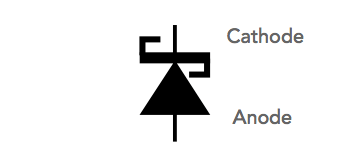
Understanding Schottky Diode Characteristics & Specifications
Although Schottky diodes share many parameters with other forms of diode, their performance is different and so are some specifications & parameters.
Home » Electronic components » this page
Schottky Barrier Diode Tutorial Includes:
Schottky barrier diode
Schottky diode technology
Schottky diode specifications
Schottky diode power rectifier
How to choose the right silicon Schottky
Silicon carbide Schottky diode
Diode types
Diode component data:
PN junction diode data
Schottky diode data
Silicon carbide, SiC Schottky diode data
Although the Schottky diode shares many of its characteristics with the more traditional forms of semiconductor diode, it still has some significant differences, and it is for these reasons that this form of diode is used within many standard electronic circuit designs, RF designs and within many power supply circuit designs.
Understanding the Schottky diode specifications and parameters helps to use them in the most effective manner in any circuit designs in which they may be used.
Selecting the right electronic component for any particular situation is key to the operation of the overall circuit design, and therefore having a good understanding of all the specifications and what they mean is important.
Basic Schottky diode characteristics
The Schottky diode is a majority carrier device, i.e. electrons in N-type material. Typically also the Schottky diodes are manufactured using N-type material as well.
This gives it a significant advantage in terms of speed because it does not rely on holes or electrons recombining when they enter the opposite type of region as in the case of a conventional diode.
In addition to this, electrons are more mobile than holes, and as most Schottky diodes are manufactured using N-type semiconductor material this further maximises the mobility.
Also by making the devices small, the normal RC type time constants can be reduced, making these diodes an order of magnitude faster than the conventional PN diodes. This factor is the prime reason why they are so popular in radio frequency applications as well as many other power applications where switching speed is important, e.g. within switching power supplies.
The Schottky diode also has a much higher current density than an ordinary PN junction. This means that forward voltage drops are much lower. This makes the diode ideal for use in power rectification applications.
The main drawback of the Schottky diode is the level of its reverse breakdown which is much lower than that of a PN diode.
Another disadvantage is the level of reverse current which is relatively high. For many uses this may not be a problem, but it is a factor which is worth watching when using it in more exacting applications.
The overall I-V characteristic is shown below. It can be seen that the Schottky diode has the typical forward semiconductor diode characteristic, but with a much lower turn on voltage. At high current levels it levels off and is limited by the series resistance or the maximum level of current injection. In the reverse direction breakdown occurs above a certain level. The mechanism is similar to the impact ionisation breakdown in a PN junction.
Schottky diode I-V characteristic
The I-V characteristic is generally that shown below. In the forward direction the current rises exponentially, having a knee or turn on voltage of around 0.2 V. In the reverse direction, there is a greater level of reverse current than that experienced using a more conventional PN junction diode.
Additionally the reverse breakdown voltage is also typically lower than an equivalent silicon PN junction diode.

The use of a guard ring included in the structure of some Schottky diodes improves its performance in both forward and reverse directions.
The main advantage of incorporating a guard ring into the structure is to improve the reverse breakdown characteristic. There is around a 4 : 1 difference in breakdown voltage between the two. Some small signal diodes without a guard ring may have a reverse breakdown of only 5 to 10 V. Whilst this may be acceptable for some low signal applications, it is not ideal for most situations.
Key Schottky diode specifications & parameters
There are several key Schottky diode specifications that need to be understood when using these diodes – they are quite different from those of a normal PN junction diode.
Although the Schottky diode exhibits many of the normal semiconductor diode parameters and specifications, there are soem that are slightly different and when using these electronic components in a circuit design, it is necessary to be aware of them.
The specifications for these diodes, like any other electronics component are normally available on the website of the manufacturer. Electronic component distributors also often have details of the specifications of components.
It is also worth noting for components that can be obtained from several manufacturers, that the specifications may vary slightly between manufacturers. For any critical parameters it is wise to use the actual figures from the manufacturer whose product is being used.
Also if a second source is being used for a particular electronic component to give a better chance of long term avalability, then the specification parameters for both manufacturers should be closely checked to ensure they meet the requirements for the particular electronic circuit design.
Forward voltage drop specification
In view of the low forward voltage drop across the diode, this is a parameter that is of particular concern. As can be seen from the Schottky diode I-V characteristic, the voltage across the diode varies according to the current being carried.
Accordingly any specification given provides the forward voltage drop for a given current. Typically the turn-on voltage is assumed to be around 0.2 V.
Reverse breakdown
Schottky diodes do not have as high a breakdown voltage as standard PN junction semiconductor diodes. Figures relating to this include the maximum Peak Reverse Voltage, maximum Blocking DC Voltage and other similar parameter names.
If these figures are exceeded then there is a possibility the diode will enter reverse breakdown and could be irreversibly damaged. It should be noted that the RMS value for any voltage will be 1/√2 times the constant value. It should also be remembered that the peak value experienced by the diode from any transient spikes should also be remembered as even short spikes will cause damage if they exceed the peak reverse voltage specification for the particular electronic component.
The upper limit for reverse breakdown is not high when compared to normal PN junction diodes. Maximum figures, even for Schottky rectifier diodes used in power supplies and similar electronic circuits may only reach around 100 V.
Schottky diode rectifiers seldom exceed this value because devices that would operate above this value even by moderate amounts would exhibit forward voltages equal to or greater than equivalent PN junction rectifiers.
Capacitance
The capacitance parameter is one of great importance for small signal RF design applications as even small values of capacitance can have a major impact on the circuit performance.
Normally the junctions areas of Schottky diodes are small and therefore the capacitance is small. Typical values of a few picofarads are normal.
As the capacitance is dependent upon any depletion areas, etc, the capacitance must be specified at a given voltage.
Reverse recovery time
This parameter is important when a diode is used in a switching application. It is the time taken to switch the diode from its forward conducting or 'ON' state to the reverse 'OFF' state.
The charge that flows within this time is referred to as the 'reverse recovery charge'. The time for this parameter for a Schottky diode is normally measured in nanoseconds, ns. Some exhibit times of 100 ps.
In fact what little recovery time is required mainly arises from the capacitance rather than the majority carrier recombination. As a result there is very little reverse current overshoot when switching from the forward conducting state to the reverse blocking state.
It was the impressive reverse recovery time specification for these electronic components that lead to their using in the famous low power Schottky series of logic integrated circuits. These 74LSxx integrated circuits were used for many years and offered improved switching time over the standard 74xx series and at a lower power level.
Reverse leakage current:
The reverse leakage parameter can be an issue with Schottky diodes. It is found that increasing temperature significantly increases the reverse leakage current parameter.
Typically for every 25°C increase in the diode junction temperature there is an increase in reverse current of an order of magnitude for the same level of reverse bias.
Working temperature:
The maximum working temperature of the junction, Tj is normally limited to between 125 to 175°C. This is less than that which can be used with ordinary silicon semiconductor diodes.
Care should be taken to ensure heatsinking of power diodes does not allow this figure to be exceeded otherwise reliability could be compromised.
Source or electronics component distributor
When deciding ona particular component for a new electronics design, it should be remembered that one major parameter is that of obtaining the electronic components.
As most components these days are obtained via an electronics component distributor, it is always worth checking on the current availability, and also gain some view of whether the components will be available in the longer term.
Fortunately for most discrete electronic components, multiple sources tend to be available, but checking the likely availability for future production as well as long term maintenance is always wise. Electronic compoennts distributors are likely to be able to advise on this, although there can obviously be no guarantees.
Schottky diode characteristics summary
The Schottky diode is used in many applications as a result of its characteristics that differ appreciable from several aspects of the more widely used standard PN junction diode.
| Schottky Diode / PN Diode Comparison | ||
|---|---|---|
| Characteristic | Schottky Diode | PN Junction Diode |
| Forward current mechanism | Majority carrier transport. | Due to diffusion currents, i.e. minority carrier transport. |
| Reverse current | Results from majority carriers that overcome the barrier. This is less temperature dependent than for standard PN junction. | Results from the minority carriers diffusing through the depletion layer. It has a strong temperature dependence. |
| Turn on voltage | Small - around 0.2 V. | Comparatively large - around 0.7 V. |
| Switching speed | Fast - as a result of the use of majority carriers because no recombination is required. | Limited by the recombination time of the injected minority carriers. |
Example Schottky diode datasheet specifications
To give some idea of the characteristics to be expected from Schottky diodes a couple of real examples are provided below. These summarise the main datasheet specifications to give an idea of their performance.
1N5828 Schottky barrier power rectifier diode
This diode is described as a Schottky diode, stud type, i.e. for power rectification. It gives an indication of how a power Schottky diode performs.
| Typical 1N5258 Shottky Diode Characteristics / Specifications | |||
|---|---|---|---|
| Characteristic | Typical Value | Unit | Details |
| Maximum recurrent peak reverse voltage | 40 | V | |
| Maxim DC blocking voltage | 40 | V | |
| Average forward current, IF (AV) | 15 | A | T = 100°C |
| Peak forward surge current, IFSM | 500 | A | |
| Maximum instantaneous forward voltage, VF | 0.5 | V | At IFM = 15A and Tj = 25°C |
| Maximum instantaneous reverse current at rated blocking voltage, IR | 10 250 |
mA | Tj= 25°C Tj = 125°C |
1N5711 Schottky barrier switching diode
This diode is described as an ultra-fast switching diode with high reverse breakdown, low forward drop voltage and a guard ring for junction protection.
| Typical 1N5711 Characteristics / Specifications | |||
|---|---|---|---|
| Characteristic | Typical Value | Unit | Details |
| Max DC Blocking Voltage, Vr | 70 | V | |
| Max forward continuous current, Ifm | 15 | mA | |
| Reverse breakdown voltage, V(BR)R | 70 | V | @ reverse current of 10µA |
| Reverse leakage current, IR | 200 | µA | At VR=50V |
| Forward voltage drop, VF | 0.41 1.00 |
V | at IF = 1.0 mA IF=15mA |
| Junction capacitance, Cj | 2.0 | pF | VR = 0V, f=1MHz |
| Reverse recovery time, trr | 1 | nS | |
Even though the examples here gives a reverse voltage characteristic of 40 V which is fairly typical, the maximum that can normally be obtained is around 100 V.
It should be noted that even though these figures are given as examples of the figures that may be expected for typical Schottky diodes, figures even for a given device number will also vary slightly between different manufacturers.
Schottky diodes are widely used in many general electronic circuit designs, RF designs, and power supply circuits. These electronic components are very useful because of their low turn on voltage, low capacitance, and fast reverse recovery times.
The components are available in standard leaded packages as well as many surface mount packages for the lower power applications. For power supply applications they are available in versions that can be bolted to heatsinks to enable the higher levels of heat to be removed.
These electronic components are widely available and there should be little problem in obtaining them from any electronics component distributor. That said, when there are general component shortages, these components will be subject to the usual delays exhibited across the range of components.
 Written by Ian Poole .
Experienced electronics engineer and author.
More Electronic Components:
Batteries
Capacitors
Connectors
ADC
DAC
Diodes
FET
Inductors
Memory types
Phototransistor
Quartz crystals
Relays
Resistors
RF connectors
Switches
Surface mount technology
Thyristor
Transformers
Transistor
Unijunction
Valves / Tubes
Return to Components menu . . .


