Schottky Diode (Schottky Barrier Diode) Explained
Schottky diodes offer low forward voltage drops and fast recovery although they have lower reverse voltage ratings and higher leakage than other diodes.
Home » Electronic components » this page
Schottky Barrier Diode Tutorial Includes:
Schottky barrier diode
Schottky diode technology
Schottky diode specifications
Schottky diode power rectifier
Silicon carbide Schottky diode
Diode types
Diode component data:
PN junction diode data
Schottky diode data
Silicon carbide, SiC Schottky diode data
The Schottky diode or Schottky Barrier diode is used in a variety of circuits where its parameters and performance enable it to provide enhanced performance over other types of diode.
The Schottky diode was one of the first types of diode ever made where it was used in the form of the Cat's Whisker rectifier for crystal radio sets in the early 1900s.
Now the diode has been developed and considerably more advanced forms are used in many areas of electronic circuit design where its properties can be used to great effect.
The Schottky diode offers many important features including very low forward voltage drop, very fast recovery times and the like. As a result the diode is used in many different types of electronic circuit design from RF detector diodes to power rectification. and much more.
Although the name used most widely for this type of diode is Schottky diode, a number of other names that may also be used. These names include surface barrier diode, Schottky barrier diode, hot carrier diode or even hot electron diode.
Operation of the Schottky barrier diode
The Schottky diode offers many advantages because it utilises a tunnelling effect to provide the diode action.
The diode consists of a metal semiconductor junction rather than a semiconductor PN junction.
The diode consists of a number of layers:
- Metal contact (cathode): The cathode contact for the diode consists of a metallic contact deposited straight onto the semiconductor.
- Lightly doped N region: The metal contact is deposited straight onto the lightly doped N region - N type semiconductor is used because electrons rather than holes are required for the tunnelling effect that gives rise to the Schottky barrier tunnelling and hence the diode.
- Heavily doped N type region: The next layer to the lightly doped N type region is a much more heavily doped region.
- Anode metal contact: The interface between the heavily doped region and the anode contact forms a bilateral contact. There is no potential to this type of contact and no rectifying action occurs. it is worth noting that when the oping level is high, there can never be a rectifying action occurring between the metal and semiconductor.
Video: Schottky DIODES: What You Really Need to Know!
To understand how the Schottky diode works, first let's look at the unbiassed state. The electrons within the metal have a high energy because they are free to roam on the metal structure. However the electrons present in the lightly doped N type semiconductor have a comparatively low level of energy. Accordingly no current flows and there is a "barrier" between them. This barrier is known as a Schottky barrier after William Schottky who discovered this form of barrier.
As the potential is increased across the diode, the electrons in the semiconductor gain sufficient energy to move across the barrier and enter the metal. They actually tunnel through the Schottky barrier and enter the metal.
The electrons that have passed through the barrier have a large amount of energy and therefore they are often referred to as "hot carriers" and as a result this type of diode have been known as a hot carrier diode.
One of the advantages of the Schottky diode is that there is no P-type material and this means that there are no holes, i.e. minority carriers. When the diode becomes reverse biassed the conduction stops very quickly and blocks the current flow. This means that there is a very rapid transition from conduction to blocking the current.
This rapid transition is very useful for switching circuits as it improves the efficiency. For example, this can result in significant improvements in the efficiency of switch mode power supply circuits.
Schottky diode circuit symbol
The circuit symbol for the Schottky diode is based around the basic diode circuit symbol. The Schottky symbol is differentiated from other types of diode by the addition of the two extra legs on the bar on the symbol.
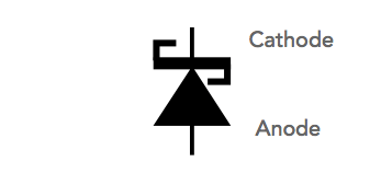
In view of the unique properties of the Schottky diode, it is important to differentiate this electronic component with the right circuit symbol as its function can be more accurately determined within any electronic circuit design.
Schottky diode advantages & disadvantages
Like any electronic component, Schottky diodes provide some distinct advantages, but there are also some disadvantages or drawbacks when using them.
When considering them for use in a given electronic circuit design, it is important to consider all aspects of their performance: both the advantages and the disadvantages.
In this way their advantages can be used to best advantage within the circuit design, while the disadvantages can be accommodated and circuit design techniques can used to overcome any issues.
In fact the advantages and disadvantages of Schottky diodes need to be carefully weighed up before selecting them for use in any particular circuit design.
Schottky diode advantages:
Low turn on voltage: The turn on voltage for the diode is between 0.2 and 0.3 volts for a silicon Schottky diode whereas a standard silicon diode has a turn on voltage of between 0.6 to 0.7 volts. This reduces resistive losses when used as a power rectifier, and enables lower signals to be detected when used as an RF detector.

VI characteristic of a Schottky diode The low turn on voltage arises because of the way the electrons tunnel through the barrier at the metal semiconductor junction.
- Low junction capacitance: Some of the RF Schottky diodes use a very small contact area. In view of the very small active area of these Schottky diodes, the capacitance levels are very small. For power diodes the active areas can be mch larger and the capacitance levels much higher.
Fast recovery time: The virtually instantaneous recovery time because current is conducted by a single type of charge carrier, i.e. the majority carriers (electrons in an N-type semiconductor). When the diode is forward-biased, these electrons are injected from the semiconductor into the metal.
When the diode is reverse-biased, there are no minority carriers to sweep out of the depletion region. Because there is no stored charge to "recover" from, the diode can switch from a conducting to a non-conducting state almost instantaneously.
The advantages of the Schottky diode, mean that its performance can far exceed that of other diodes in many areas.
Schottky diode disadvantages:
Low reverse breakdown voltage: Schottky diodes or Schottky barrier diodes are well known for having only a low reverse breakdown voltage. Figures may even be as low as 50 V for some power diodes, although voltages p to 200V and a little beyond are typically the maximum for silicon diodes
If higher reverse breakdown voltages are required, then silicon carbide, SiC Schottky diodes should be considered. These can offer reverse breakdown voltages of over 1 kV for the right device.
High leakage current: Another feature of Schottky diodes is the high reverse leakage levels that occur across a Schottky junction.
Schottky diode applications
The Schottky barrier diodes are widely used in the electronics industry finding many uses as diode rectifier. Its unique properties enable it to be used in a number of applications where other diodes would not be able to provide the same level of performance. In particular it is used in areas including:
RF mixer and detector diode: The Schottky diode is a very useful component for radio frequency applications because of its high switching speed and high frequency capability. In view of this Schottky barrier diodes are used in many high performance diode ring mixers. In addition to this the low turn on voltage in addition to the low junction capacitance makes this type of diode ideal for use in RF detectors.

A double balanced mixer circuit often uses Schottky diodes Power rectifier: Schottky diodes are also used as high power rectifiers. Their high current density and low forward voltage drop mean that less power is wasted than if ordinary PN junction diodes were used. This increase in efficiency means that less heat has to be dissipated, and smaller heat sinks can be used, thereby saving weight and cost.
Power OR circuits: Schottky diodes can be used in applications where a load is driven by two separate power supplies. One example may be a mains power supply and a battery supply. In these instances it is necessary that the power from one supply does not enter the other. This can be achieved using diodes. However it is important that any voltage drop across the diodes is minimised to ensure maximum efficiency. As in many other applications, this diode is ideal for this in view of its low forward voltage drop.
Schottky diodes tend to have a high reverse leakage current. This can lead to problems with any sensing circuits that may be in use. Leakage paths into high impedance circuits can give rise to false readings. This must therefore be accommodated in the circuit design.
Solar cell applications: Solar cells are typically connected to rechargeable batteries, often lead acid batteries because power may be required 24 hours a day and the Sun is not always available. Solar cells do not like the reverse charge applied and therefore a diode is required in series with the solar cells. Any voltage drop will result in a reduction in efficiency and therefore a low voltage drop diode is needed. As in other applications, the low voltage drop of the Schottky diode is particularly useful, and as a result they are the favoured form of diode in this application.
Clamp diode: Schottky barrier diodes may also be used as a clamp diode in a transistor circuit to speed the operation when used as a switch. Years ago they found widespread use in this application, forming a key element in the 74LS (low power Schottky) and 74S (Schottky) families of logic circuits. When used in this manner the Schottky diodes are inserted between the collector and base of the driver transistor to act as a clamp. To produce a low or logic "0" output the transistor is driven hard on, and in this situation the base collector junction in the diode is forward biased. When the Schottky diode is present this takes most of the current and allows the turn off time of the transistor to be greatly reduced, thereby improving the speed of the circuit.

An NPN transistor with Schottky diode clamp
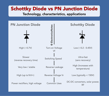
Comparison of the Schottky diode vs PN junction diode
There are several differences between Schottky diodes and PN junction diodes in their structure and also in their operation, characteristics and as a result in their applications.
The infographic below, provides a summary of their differences.
The Schottky diode or Schottky barrier diode is used in many applications. It is unusual in that it is used for both very low power signal detection and also for high power rectification. The properties of the Schottky diode make it idea for use at both ends of the spectrum.
The Schottky diode is also used within a number of other devices from photodiodes to MESFETs. In this way, not only does this form of diode find uses in many circuits in its discrete format, but it is also an essential part of many other components and technologies as well.
 Written by Ian Poole .
Experienced electronics engineer and author.
More Electronic Components:
Batteries
Capacitors
Connectors
ADC
DAC
Diodes
FET
Inductors
Memory types
Phototransistor
Quartz crystals
Relays
Resistors
RF connectors
Switches
Surface mount technology
Thyristor
Transformers
Transistor
Unijunction
Valves / Tubes
Return to Components menu . . .