Surface mount devices, SMDs, or SMT components come in a variety of packages. As virtually all mass produced electronics uses surface mount technology: surface mount components are of great importance
These surface mount components come in a variety of packages, most of which are standardised to make the manufacture of the PCB assemblies using automated equipment much easier.
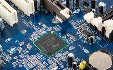
Printed circuit board with a variety of SMT packages as well as through hole mounted connectors
Some of the most widely used components are surface mount resistors and surface mount capacitors. These SMD resistors and capacitors these come in small rectangular packages, some of which are absolutely minute.
Additionally there is a variety of different SMT packages for integrated circuits dependent upon the level of interconnectivity required, the technology being used and a variety of other factors.
A number of other components are available, some of which are in standard packages, but others, because of their very nature need specialised packages with non-standard outlines.
Requirements for PCB component handling
When the surface mount packages were developed, one of the considerations that was given was that of component handling. As the whole aim of surface mount technology was that it should facilitate automated PCB assembly, the packages needed to be designed so that they could be manipulated on pick and place machines easily.
The SMT package styles have been developed to provide easy handling during the shipping and stock stages of the supply chain, and then by the pick and pale machines used for PCB assembly.
Ensuring the components can be handled easily at all stages, ensures that manufacturing costs are reduced, and the quality of the assembled PCBs and the final equipment is as high as possible.
Often the very smallest components are held loose in a hopper and these are fed down a tube and picked out as required.
Larger surface mount components like resistors and capacitors as well as many surface mount diodes and transistors may be held in a tape on a reel. The reel consists of a tape within which the components are held and a second tape is loosely stuck onto the back As the machine uses components, so the retention tape is pulled off exposing the next component to be used.
Other components like dual in line surface mount ICs may be held in a tube from which they can be removed as required, and then under gravity the next one slides down.
Very large ICs, possibly quad flat packs, QFPs and plastic leaded chip carriers, PLCCs may be held in what is called a waffle pack which is placed onto the pick and place machine. Components are successively removed as they are required.
JEDEC SMT package standards
Industry standards are used to provide a large degree of conformity across the industry. Accordingly the sizes of most SMT components conform to industry standards like the JEDEC specifications.
The JEDEC Solid State Technology Association is an independent semiconductor engineering trade organisation and standardisation body. The organisation has over 300 member companies, many of which are some of the largest electronics companies.The letters JEDEC stand for Joint Electron Device Engineering Council, and as the name indicates it manages and develops many standards associated with semiconductor devices of all types. One aspect of this is the surface mount technology component packages.
Obviously different SMT packages are used for different types of components, but the fact that there are standards enables activities such as printed circuit board design to be simplified as standard pad sizes and outlines can be prepared and used.
Additionally the use of standard size packages simplifies the manufacture because pick and place machines can use standard feed for the SMT components, considerably simplifying the manufacturing process and saving costs.
The different SMT packages can be categorised by the type of component, and there are standard packages for each.
Passive rectangular components
Passive surface mount devices are mainly comprised of SMD resistors and SMD capacitors. There are several different standard sizes which have been reduced as technology has enabled smaller components to be manufactured and used
It will be seen that the devices size names are derived from their measurements in inches.
Common Passive SMD Package Details
SMD Package type
Dimensions mm
Dimensions inches
2920
7.4 x 5.1
0.29 x 0.20
2725
6.9 x 6.3
0.27 x 0.25
2512
6.3 x 3.2
0.25 x 0.125
2010
5.0 x 2.5
0.20 x 0.10
1825
4.5 x 6.4
0.18 x 0.25
1812
4.6 x 3.0
0.18 x 0.125
1806
4.5 x 1.6
0.18 x 0.06
1210
3.2 x 2.5
0.125 x 0.10
1206
3.0 x 1.5
0.12 x 0.06
1008
2.5 x 2.0
0.10 x 0.08
0805
2.0 x 1.3
0.08 x 0.05
0603
1.5 x 0.8
0.06 x 0.03
0402
1.0 x 0.5
0.04 x 0.02
0201
0.6 x 0.3
0.02 x 0.01
01005
0.4 x 0.2
0.016 x 0.008
Of these sizes, the 1812, and 1206 sizes are now only used for specialised components or ones requiring larger levels of power to be dissipated The 0603 and 0402 SMT sizes are the most widely used, although with miniaturisation moving forwards, 0201 and smaller SMD resistors and capacitors are being used increasingly.
When using surface mount resistors, care must be taken to ensure that the power dissipation levels are not exceeded as the maximum figures are much less than for most leaded resistors
Note on the Surface Mount Capacitors:
Small surface mount capacitors are used by the billion in all forms of mass produced electronic equipment. Surface mount capacitors are nomally small rectangular cuboids the dimesnions of which normally manufactured to conform to the industry standard sizes. SMCD capacitors may use a variety of technologies including multilayer ceramic, tantalum, electrolytic and some other less widely used varieties.
Surface mount technology offers significant advantages for the mass production of electronic equipment. Small surface mount resistors are used by the billion in all forms of mass produced electronic equipment. Resistors are typically very small cuboid devices and they are normally manufactured to conform to the industry standard sizes
Although the main use for these sizes surface mount component packages is for SMD resistors and SMD capacitors, they are also used for some other other components. In some cases it is not physically possible to adopt these standard sizes, but some other components do use them. One example is that is SMD inductors. Naturally it is very difficult for the very smallest sizes, but SMD inductors are available in 0805 and 0603 sizes.
Tantalum capacitors SMD packages
As a result of the different construction and requirements for tantalum SMT capacitors, there are some different packages that are used for them. These conform to EIA specifications.
Common SMD Tanatalum Capacitor Package Details
SMD Package type
Dimensions mm
EIA standard
Size A
3.2 x 1.6 x 1.6
EIA 3216-18
Size B
3.5 x 2.8 x 1.9
EIA 3528-21
Size C
6.0 x 3.2 x 2.2
EIA 6032-28
Size D
7.3 x 4.3 x 2.4
EIA 7343-31
Size E
7.3 x 4.3 x 4.1
EIA 7343-43
Other passive SMD components
There are several types of other component that are not able to adopt the standard surface mount component sizes used by the majority of SMD resistors and capacitors.
Surface mount versions of components like many types of inductor, transformers, quartz crystal resonator, temperature controlled crystal oscillators TCXOs, filters, ceramic resonators and the like may require different style packages, often larger than the ones that are sued for surface mount resistors and capacitors.
These packages are unlikely to adopt the standard surface mount component package sizes in view of the unique nature of the components.
Whatever the package style chosen it must be able to fit the automated PCB assembly processes and be handled by a pick and place machine.
Transistor & diode packages
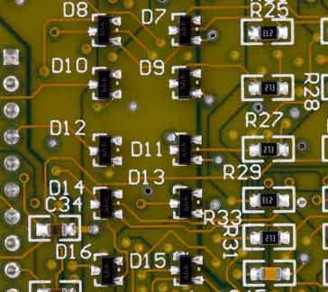
SMD transistors and diodes often share the same types of package. While diodes only have two electrodes a package having three enables the orientation to be correctly selected.
SMT / SMD diodes on a printed circuit board
Although a variety of SMT transistor and diode packages are available, some of the most popular are given in the list below.
SOT-23 - Small Outline Transistor: The SOT23 SMT package is the most common outline for small signal surface mount transistors. The SOT23 has three terminals for a diode of transistor, but it can have more pins when it may be used for small integrated circuits such as an operational amplifier, etc. It measures 3 mm x 1.75 mm x 1.3 mm.
SOT-223 - Small Outline Transistor: The SOT223 package is used for higher power devices like higher power surface mount transistors or other surface mount devices. It is larger than the SOT-23 and it measures 6.7 mm x 3.7 mm x 1.8 mm. There are generally four terminals, one of which is a large heat-transfer pad. This enables heat to be transferred to the printed circuit board.
Integrated circuit SMD packages
There are many forms of package that are used for surface mount ICs. Although there is a large variety, each one has the areas where its use is particularly applicable.
SOIC - Small Outline Integrated Circuit : This surface mount IC package has a dual in line configuration and gull wing leads with a pin spacing of 1.27 mm
SOP - Small Outline Package: There are several versions of this SMD package:
TSOP - Thin Small Outline Package: This surface mount IC package is thinner than the SOIC and has a smaller pin spacing of 0.5 mm
SSOP - Shrink Small Outline Package: This package has a pin spacing of 0.635 mm
TSSOP - Thin Shrink Small Outline Package:
QSOP - Quarter-size Small Outline Package: It has a pin spacing of 0.635 mm
VSOP - Very Small Outline Package: This is smaller than the QSOP and has pin spacing of 0.4, 0.5, or 0.65 mm.
QFP- Quad flat pack: The QFP is the generic type of flat package for surface mount ICs. There are several variants as detailed below.
LQFP - Low profile Quad Flat Pack: This package has pins on all four sides. Pin spacing varies according to the IC, but the height is 1.4 mm.
PQFP - Plastic Quad Flat Pack: A square plastic package with equal number of gull wing style pins on each side. Typically narrow spacing and often 44 or more pins. Normally used for VLSI circuits.
CQFP - Ceramic Quad Flat Pack: A ceramic version of the PQFP.
TQFP - Thin Quad Flat Pack: A thin version of the PQFP.
The quad flat pack package for surface mount ICs has the very thin gull wing leads coming out of all sides. On high pin count surface mount ICs, these can be very thin and easily bent. Once bent they are almost impossible to reform into the required positions. Great care must be taken int he PCB assembly process when handling these devices.
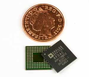
BGA - Ball Grid Array: The ball grid array SMD package has all its contact pads underneath the device package. Before soldering the pads appear as solder balls, giving rise to the name. SMB BGA package showing top and undersides
Placing the contacts underneath the device reduces the area required whilst maintaining the number of connections available. This format also overcomes some of the problems of the very thin leads required for the quad flat packs and makes the package physically more robust. The ball spacing on BGAs is typically 1.27 mm.
When the BGA package was first introduced, doubts existed in many quarters about the reliability of soldering of the contact points under the package, but when the PCB assembly process is operating correctly, there are no issues.
Although there appear to be very many different SMD packages, the fact that there are standards reduces the number and it is possible to set up printed circuit board design packages to accommodate them, along with proven pad sizes on the boards. In this way the packages enable high quality printed circuit board assembly and the reduction in overall number of variables within a design.
Written by Ian Poole . Experienced electronics engineer and author.

 Written by Ian Poole .