Phototransistors vs Photodiodes: Choosing the Right Sensor for Your Light-Detection Application
This comprehensive guide details the technological differences between photodiodes and phototransistors, looking at their relative advantages and disadvantages, and the different applications for each.
Home » Electronic components » this page
Phototransistor Includes:
Phototransistor basics
Applications & circuits
Photodiode vs phototransistor
Photodarlington
Optocoupler / optoisolator
In the world of electro-optics, the detection of light is the first and often most critical step in countless applications, from smoke detectors and barcode scanners to fiber-optic communications and medical imaging.

At the heart of this detection process are solid-state semiconductor sensors, primarily the photodiode and the phototransistor.
While both convert light energy into electrical current, their internal mechanisms, performance characteristics, and ideal applications differ profoundly.
Understanding the Core Technology: Light-to-Electricity Conversion
To understand the operational differences between the photodiode and the phototransistor, one must first appreciate the underlying physics of how each device interacts with photons. Both are based on semiconductor $p$-$n$ junctions, but the way they use the photogenerated current is the key differentiator.
The Photodiode: A Precision Current Source
A photodiode is essentially a PN junction operated in reverse-bias mode.
When a photon with sufficient energy strikes the depletion region of the junction, it excites an electron, creating an electron-hole pair.
The strong electric field across the reverse-biased junction quickly sweeps these carriers apart — the electrons drift to the N-side and the holes to the P-side.
This generates a tiny current proportional to the incident light intensity. This current is known as the photocurrent (Iλ).
Key Operational Modes:
Photovoltaic Mode (Zero Bias): Used in solar cells or very low-light precision applications. The diode generates a voltage proportional to light, but the response is non-linear and slower.
Photoconductive Mode (Reverse Bias): The most common mode for sensing. Applying a reverse voltage increases the size of the depletion region, reducing junction capacitance (Cj) and making the device much faster and its response linear. The output is a small current that requires an external transimpedance amplifier (TIA) for practical use.
The Phototransistor: A Photodiode with Integrated Gain
A phototransistor is structurally a standard bipolar junction transistor (BJT) — either NPN or PNP, but with one critical modification: the base terminal is typically left electrically unconnected and is exposed to light.
In a phototransistor, the collector PN junction junction acts exactly like a photodiode. When photons strike this junction, they generate a primary photocurrent (Iλ). However, instead of being the final output, this small Iλ current is fed directly into the base of the transistor.
The base current is then internally amplified by the transistor's current gain (beta, or hFE).
This inherent current gain means the phototransistor provides a much larger electrical output signal for the same amount of incident light compared to a photodiode, often eliminating the need for complex external amplification circuitry.
Relative Advantages: Sensitivity vs. Speed and Linearity
The core difference—the internal gain of the phototransistor—leads to a clear trade-off between the two technologies: Sensitivity vs. Speed.
The Photodiode’s Superiority in Speed and Linearity
The photodiode's principal advantage is its exceptional speed and bandwidth.
• Typical photodiode applications summary
| Advantage | Explanation | Consequence |
|---|---|---|
| High Speed / Low Capacitance | Since a photodiode operates solely by carrier drift across the reverse-biased depletion region, it has very low junction capacitance (Cj). The response time is typically in the nanosecond (ns) range. | Essential for high-speed data transmission (e.g., fiber optics) and timing-critical laser systems. |
| Excellent Linearity | The output photocurrent is extremely proportional to incident light intensity over several decades. This predictability is maintained even at high frequencies. | Ideal for radiometry and precision metrology where accurate measurement of absolute light intensity is required. |
| Low Noise | The photodiode’s minimal output current has a very low and predictable noise floor. With a high-quality external transimpedance amplifier (TIA), the signal-to-noise ratio (SNR) can be exceptionally high. | Allows for accurate detection of extremely weak light or small signal changes superimposed on a large background. |
| Broad Wavelength Range | By varying the semiconductor material (e.g., Silicon, Germanium, InGaAs), photodiodes can be optimized to detect light from the deep ultraviolet (UV) to the mid-infrared (IR). | Highly versatile for spectrally selective applications like medical analyzers or chemical sensing. |
The Phototransistor’s Advantage in Sensitivity and Simplicity
The phototransistor's internal current gain gives it a distinct lead in applications prioritizing signal strength and simplicity.
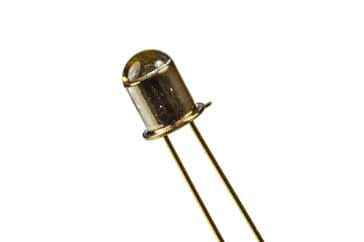
Note the lens at the top and the fact that it only has two leads because the base is often left open circuit and no external connection is provided.
• Typical applications summary
| Advantage | Explanation | Consequence |
|---|---|---|
| High Sensitivity (High Responsivity) | The internal current gain (β), which can range from 100 to over 1000, multiplies the initial primary photocurrent (Iλ) from the collector-base junction. | Ideal for low-light conditions or applications where the sensor is placed far from the light source (e.g., long-distance remote control). |
| Simpler Circuitry | Due to the high output current, the phototransistor can often directly drive a load or interface with digital logic without a dedicated amplification stage. | This eliminates the need for a dedicated external amplifier (TIA), reducing component count, cost, and complexity. |
| Lower System Cost | While the component cost may be comparable, the removal of the need for complex, precise external amplifier circuits reduces the cost of the overall system design and bill of materials (BOM). | Favoured in mass-market, consumer, and high-volume industrial applications where cost minimization is critical. |
| High Current Output | The amplified collector current can be in the milliamp (mA) range, allowing it to directly activate low-power loads. | Useful for optically coupled relays or simple light-activated on/off switching tasks triggered by light. |
 Written by Ian Poole .
Experienced electronics engineer and author.
More Electronic Components:
Batteries
Capacitors
Connectors
ADC
DAC
Diodes
FET
Inductors
Memory types
Phototransistor
Quartz crystals
Relays
Resistors
RF connectors
Switches
Surface mount technology
Thyristor
Transformers
Transistor
Unijunction
Valves / Tubes
Return to Components menu . . .