Understanding Op-Amp CMRR: Calculations, Frequency Limits & Design Tips
Discover how Operational Amplifier CMRR rejects noise, why it drops at high frequencies, and how to maximize circuit performance.
Op-amp Tutorial Includes:
Introduction
Op amp gain
Bandwidth
Op amp slew rate
Offset null
Input impedance
Output impedance
Current feedback op amp
Understanding specifications
Common mode rejection ratio, CMRR
How to choose an op amp
Op amp circuits summary
Operational amplifiers (op-amps) are fundamental building blocks in modern analogue electronics.
Whether utilized in delicate sensor signal conditioning, audio processing systems, or precision instrumentation circuits, an op-amp is fundamentally designed as a differential amplifier.
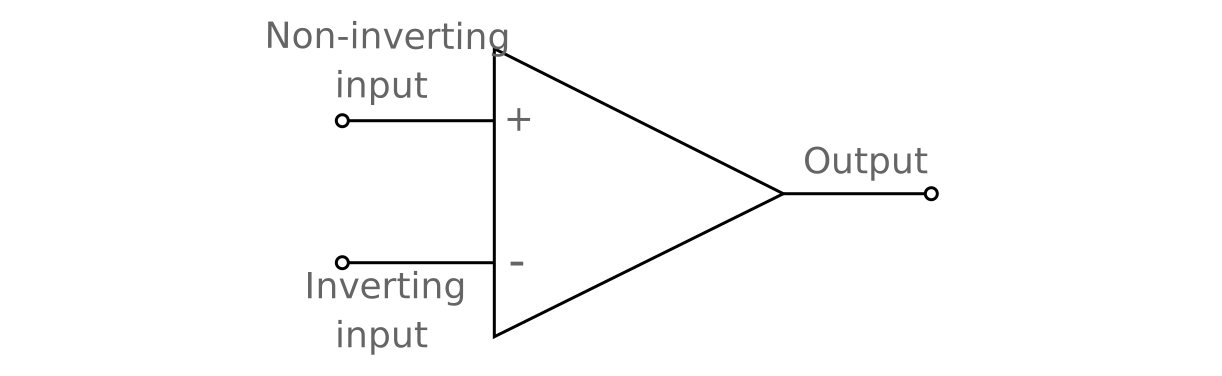
Its core function is to amplify the voltage difference between its two input terminals—the inverting input (−) and the non-inverting input (+)—while ignoring any signal that is common to both.
In real-world applications, however, no operational amplifier is perfect. Undesired signals such as power line hum, radio frequency interference (RFI), and ground noise frequently appear equally on both input lines.
The parameter that quantifies an op-amp's ability to reject these unwanted, shared signals is known as the Common Mode Rejection Ratio (CMRR). Understanding CMRR, how it is calculated, its frequency dependency, and how external components impact performance is vital for designing robust high-precision electronics.
Understanding Differential vs. Common Mode Signals
To understand Common Mode Rejection Ratio, one must first distinguish between the two types of input voltages present at an op-amp’s input terminals: differential mode voltages and common mode voltages.
1. Differential Mode Voltage (VDIFF)
The differential input signal is the difference between the voltages applied to the non-inverting terminal (V+) and the inverting terminal (V−):
VDIFF = V+ − V−
The primary role of an op-amp is to amplify this differential voltage by a differential open-loop gain, denoted as AVD (or simply AD). The resulting differential output contribution is:
VOUT_DIFF = AVD × (V+ − V−)
2. Common Mode Voltage (VCM)
The common mode signal represents the average voltage level present simultaneously at both input terminals with respect to circuit ground:
VCM = (V+ + V−) / 2
In an ideal operational amplifier, a voltage applied equally to both inputs results in zero output voltage. However, real-world internal asymmetries—such as minor transistor mismatch in the input differential pair—cause the op-amp to amplify this shared voltage slightly. This amplification factor is known as the common mode gain, ACM.
The total output voltage of a real op-amp is therefore the sum of both differential and common mode contributions:
VOUT = (AVD × VDIFF) + (ACM × VCM)
Defining Common Mode Rejection Ratio (CMRR)
The Common Mode Rejection Ratio measures the ratio of the differential gain to the common mode gain. Mathematically, it expresses how much more strongly the amplifier responds to differential signals compared to common mode signals.
As a raw dimensionless ratio, CMRR is defined as:
CMRR (Ratio) = | AVD / ACM |
Because op-amps are designed to have extremely high differential gain and very low common mode gain, this ratio is typically very large. Consequently, CMRR is almost universally expressed in decibels (dB):
CMRR (dB) = 20 × log10 (| AVD / ACM |)
A higher CMRR figure indicates a superior operational amplifier capable of suppressing unwanted common mode noise while faithfully amplifying the signal of interest.
• An Example Calculation
Consider an operational amplifier with an open-loop differential voltage gain (AVD) of 100,000 (100 dB) and a common mode gain (ACM) of 0.1 (−20 dB). The CMRR is calculated as:
CMRR = 100,000 / 0.1 = 1,000,000
Expressed in decibels:
CMRR (dB) = 20 × log10(1,000,000) = 120 dB
This means the amplifier is one million times more sensitive to differential signals than to common mode noise.
Why CMRR Matters in Engineering Applications
In practical measurement environments, common mode noise is nearly unavoidable. Understanding CMRR is critical in several key hardware scenarios:
Instrumentation and Sensor Measurement: Transducers like strain gauges, thermocouples, and Wheatstone bridges often output microvolt or millivolt-level differential signals riding on a baseline common mode voltage of several volts. A low CMRR causes the common mode baseline to mask the tiny sensor readings.
One example of using operational amplifiers to provide high gain for small differential signals is with strain gauges like the one shown below.
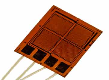
Example of a Wheatstone full bridge strain gauge
A differential amplifier like an operational amplifier is typically used to amplify the small difference signals from strain gauges like this one /figcaption>- Biomedical Signal Acquisition: Equipment such as Electrocardiograms (ECG) and Electroencephalograms (EEG) measure biological potentials in the millivolt range. The human body acts as an antenna picking up 50 Hz/60 Hz mains hum from surrounding electrical wiring. Strong common mode rejection is essential to prevent mains interference from distorting cardiac or brainwave traces.
- Current Sensing Applications: High-side current sensing requires measuring a small voltage drop across a sense resistor connected to a high DC supply line. The high supply voltage constitutes a large common mode signal; without high CMRR, small current variations cannot be accurately measured.
- Long-Distance Audio and Communications: Balanced audio lines (using XLR cables) carry inverted signals across two conductors surrounded by a common shield. Any electromagnetic interference picked up along the cable path affects both conductors identically. A high-CMRR differential receiver cancels out this induced noise completely.
CMRR Frequency Dependency and Performance Degradation
Datasheet specifications for CMRR often highlight impressive figures—such as 100 dB to 140 dB—at direct current (DC) or low frequencies. However, engineers must recognize that CMRR drops significantly as signal frequency increases.
This drop occurs primarily because the open-loop differential gain (AVD) decreases with frequency due to internal compensation capacitors used to ensure amplifier stability. Meanwhile, internal stray capacitances and mismatch across the input stage cause the common mode gain (ACM) to increase at higher frequencies.
A typical CMRR vs. Frequency curve exhibits a flat response from DC up to a corner frequency (often between 10 Hz and 1 kHz), after which it rolls off at a rate of approximately −20 dB per decade.
| Frequency Band | Typical CMRR Range | Primary Limiting Factors |
|---|---|---|
| DC to Low Frequency (< 100 Hz) | 90 dB to 130 dB | Transistor matching, DC bias tail current source impedance. |
| Medium Frequency (1 kHz – 10 kHz) | 60 dB to 90 dB | Dominant pole roll-off of internal open-loop gain (AVD). |
| High Frequency (> 100 kHz) | 20 dB to 50 dB | Parasitic capacitance imbalances and slew rate limitations. |
Because of this degradation, an op-amp configured for high performance at 50 Hz mains hum may offer significantly less rejection against high-frequency switching noise originating from modern switch-mode power supplies (SMPS) or digital clock networks.
The Critical Impact of External Resistor Matching
While an operational amplifier's intrinsic CMRR is fixed during silicon fabrication, the overall CMRR of a closed-loop amplifier circuit is heavily controlled by the precision of surrounding passive components.
Consider a standard four-resistor difference amplifier circuit configured with input resistors R1 and R2, and feedback/ground resistors R3 and R4. The ideal differential output equation assumes perfect resistor matching where R3/R1 = R4/R2.
If there is even a minor mismatch in these resistor ratios, common mode voltage is converted directly into a differential error voltage. The overall circuit CMRR (CMRRTOTAL) can be approximated by combining the op-amp's intrinsic CMRR (CMRROPAMP) and the CMRR contribution due to resistor tolerances (CMRRRESISTORS):
1 / CMRRTOTAL ≈ (1 / CMRROPAMP) + (1 / CMRRRESISTORS)
For a basic difference amplifier with an intended unity gain, the worst-case CMRR due purely to resistor tolerance (ε) is approximated by:
CMRRRESISTORS ≈ (1 + ACLOSED_LOOP) / (4 × ε)
Where ε is the fractional tolerance of the resistors (e.g., ε = 0.01 for 1% resistors):
- 1% Resistors (ε = 0.01): Maximum achievable circuit CMRR is roughly 50 (34 dB), regardless of whether the underlying op-amp boasts a 120 dB spec sheet!
- 0.1% Resistors (ε = 0.001): Maximum achievable circuit CMRR improves to roughly 500 (54 dB).
- 0.01% Resistors (ε = 0.0001): Circuit CMRR improves to roughly 5,000 (74 dB).
This highlights a key rule in analogue system design: High-performance operational amplifiers require precision-matched resistor networks to realize their full common mode rejection capabilities. For demanding applications, engineers often select integrated Instrumentation Amplifiers (InA), which feature laser-trimmed internal resistor networks capable of achieving overall circuit CMRRs well in excess of 100 dB.
Measuring and Testing CMRR
To verify the Common Mode Rejection Ratio experimentally, engineers use dedicated test configurations to avoid accuracy errors caused by equipment limitations.
A simple measurement approach involves applying a known AC or DC common mode voltage (VCM) simultaneously to both inputs tied together and measuring the resulting output voltage (VOUT). The common mode gain is calculated as ACM = VOUT / VCM. Combined with the open-loop differential gain AVD from the datasheet, CMRR can be derived.
However, because measuring extremely small output changes against large differential gains can introduce measurement error, standardized testing often utilizes a specialized closed-loop test circuit with an auxiliary amplifier. This setup forces the common mode voltage to fluctuate while keeping the device-under-test (DUT) operating in a stable linear region, allowing accurate measurement of input offset voltage shift (ΔVOS) relative to common mode voltage shift (ΔVCM):
CMRR = ΔVCM / ΔVOS
Expressed in decibels:
CMRR (dB) = 20 × log10 (ΔVCM / ΔVOS)
Design Guidelines for Maximising Circuit CMRR
Achieving optimal common mode rejection requires careful design choices across schematic design, component selection, and printed circuit board (PCB) layout:
- Use Integrated Instrumentation Amplifiers: When high CMRR is required for low-level differential signal processing, use a dedicated 3-op-amp or 2-op-amp instrumentation amplifier rather than constructing a difference amplifier with discrete resistors.
- Specify High-Precision Resistor Networks: If discrete difference amplifiers are mandatory, select matched resistor networks on a single substrate rather than individual discrete precision resistors to ensure tight ratio tracking over temperature changes.
- Maintain Symmetry in PCB Routing: Ensure differential input lines are routed symmetrically with equal trace lengths, identical widths, and balanced impedance paths. Differential pairs should be guarded by continuous ground planes to prevent unequal noise pickup.
- Account for Parasitic Capacitance: Unequal stray capacitance on the input lines degrades high-frequency CMRR by introducing differential phase shifts. Keep trace lengths short and balance input filter capacitors carefully.
- Filter High-Frequency Common Mode Noise: Implement matched common mode RC low-pass filters or common mode chokes at the input stage to attenuate high-frequency interference before it reaches the op-amp inputs.
Conclusion
Common Mode Rejection Ratio is a vital figure of merit for operational amplifiers, governing their ability to isolate small differential signals from pervasive background noise and DC offsets. While a high DC CMRR specification on a datasheet provides a solid baseline, real-world system performance depends on the frequency spectrum of the noise, the precision of external passive components, and PCB layout symmetry. By understanding these mechanisms, analogue designers can engineer robust, high-precision measurement systems capable of extracting clean signals from noisy environments.
 Written by Ian Poole .
Experienced electronics engineer and author.
More Circuits & Circuit Design:
Op Amp basics
Op Amp circuits
Power supply circuits
Transistor design
Transistor Darlington
Transistor circuits
FET circuits
Circuit symbols
Return to Circuit Design menu . . .