How to Choose the Right Schottky Diode for Your Circuit Design
Understand the key decisions and options when selecting a Schottky diode for your circuit design - from my experience I explain the options, advantages and disadvantages that need to be considered.
Home » Electronic components » this page
Schottky Barrier Diode Tutorial Includes:
Schottky barrier diode
Schottky diode technology
Schottky diode specifications
Schottky diode power rectifier
How to choose the right silicon Schottky
Silicon carbide Schottky diode
Diode types
Diode component data:
PN junction diode data
Schottky diode data
Silicon carbide, SiC Schottky diode data
When designing any circuit, there are many decisions to make and these often require skill and expertise to gain the right balance between several factors.
Choosing the right Schottky barrier diode is a classic example of balancing interdependent trade-offs.
This page focusses on the traditional silicon Schottky diodes, but of course, Silicon Carbide Schottky's are also available and are the ideal choice for many applications.
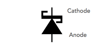
For design engineers working on high-frequency power supplies, reverse polarity protection, or low-voltage power OR-ing rails, the Schottky diode is an indispensable tool. Its distinct lack of a standard p-n junction gives it two legendary properties: an exceptionally low forward voltage drop (VF) and near-zero reverse recovery time (trr).
but there are disadvantages to using these diodes as well. Silicon Schottky diodes have a high reverse leakage, and this is even worse at high temperatures.
Another disadvantage is that their maximum reverse voltage blocking capability (VRRM) tops out around 200V for the highest voltage diodes and for many it is very much less.
1. The Physics Brief: Why It Matters to the Circuit
To select the right component, we must first look at how a Schottky diode behaves under the hood. Traditional rectifiers rely on a p-n semiconductor junction where minority charge carriers must recombine when switching from a forward-biased state to a reverse-biased state. This recombination takes time, manifesting as a reverse recovery current spike (IRM) and a corresponding time delay (trr).
A Schottky diode replaces the p-type element of the junction with a metal contact (typically molybdenum, platinum, chromium, or tungsten) bonded to an n-type silicon substrate.
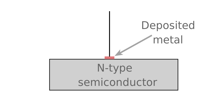
Note, real diodes typically have a more complicated structure to improve performance and reduce breakdown
As a result of the fact that the current is carried almost entirely by majority carriers, i.e. electrons in the conduction band, there is virtually no stored minority carrier charge.
When the voltage flips, the current shuts off near-instantaneously. The "switching loss" seen in a silicon Schottky datasheet isn't caused by carrier recombination; it is almost entirely the result of charging and discharging the device's parasitic junction capacitance (CJ).
2. Core electrical parameters demystified
When looking at a datasheet for a classic part like an MBR340, SS14, or a high-current trench Schottky, it is really important to look at how parameters shift under real-world operating conditions.
Maximum Repetitive Reverse Voltage (VRRM)
This is the absolute maximum peak voltage the diode can block in its off-state.
The Engineering Rule: Never run a silicon Schottky right at its VRRM limit. High-frequency circuits inherently suffer from inductive voltage spikes during switching transitions.
he Recommendation: Often design recommendations suggest a safety margin of at least 20% to 30% above your maximum steady-state DC rail. I personally prefer to run things with a 40% margin, i.e. at a maximum of 60% of the design maximum ratings. If you are rectifying a 24V rail that sees transient spikes up to 32V, a 40V or 45V rated diode (VRRM) is the bare minimum; a 60V device is significantly much safer, and there is often little cost difference.
Forward Voltage Drop (VF)
The headline feature of the Schottky is a low VF, typically between 0.2V and 0.5V, compared to 0.7V to 1.1V for standard silicon p-n diodes. (Although the turn on voltage is typically 0.2V for Schottky diodes and 0.6 to 0.7V for standard silicon diodes, when current passes through the overall voltage drop is actually higher).
The Nuance: VF is composed of two distinct parts: the ideal barrier voltage and the internal series resistance (RD) of the silicon substrate multiplied by the forward current (IF). At low currents, the barrier voltage dominates. At high currents, the ohmic voltage drop across RD takes over, causing the VF curve to steepen significantly.
Temperature Dependency: Crucially, VF features a negative temperature coefficient. As the junction temperature (TJ) increases, VF drops. While this slightly improves conduction efficiency at high loads, it directly worsens the next parameter.
Reverse Leakage Current (IR)
The reverse leakage current is one of the major disadvantages of Schottky diodes and in some instances it can mean that silicon Schottky diodes are not able to be used.
While a standard p-n diode might leak a few nanoamps or microamps under reverse bias, a silicon Schottky can easily leak hundreds of microamps at room temperature (25°C).
The Temperature Trap: IR scales exponentially with temperature. A Schottky leaking 10µA at room temperature can easily leak 10 mA to 50 mA when running hot at 125°C. This leakage represents a major source of standby power dissipation and introduces the real danger of thermal runaway.
Average Rectified Forward Current (IF(AV)) and Surge Current (IFSM)
IF(AV): The maximum average current the diode can sustain continuously over a complete cycle, usually specified under a specific thermal environment (e.g., a specific PCB copper pad area or lead temperature).
IFSM: The non-repetitive peak surge current the device can handle for a brief window (typically a single half-sine wave pulse at 50Hz or 60Hz). This is critical for circuits charging large input bulk capacitors at startup, where inrush currents can be orders of magnitude higher than nominal operating currents.
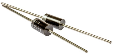
3. The interdependent trade-offs
As with many engineering decisions, there is a real balance between the different options available.
When manufacturers optimize a silicon Schottky diode, they have to tune the thickness of the epi-layer and choose the barrier metal.
This sets off a cascade of architectural trade-offs that must be considered and the engineer needs to balance the eprformance during component selection:
| |
|||
|---|---|---|---|
| Component Option | Forward Voltage VF | Reverse leakagae | Impact on Reverse Voltage VRRM |
| Low-Barrier Metal | Ultralow VF (0.2V – 0.35V) | Very high leakage current | Limited to lower voltages (≤ 30V) |
| High-Barrier Metal | Moderate VF (0.45V – 0.6V) | Low leakage current | Higher voltage blocking (40V – 100V+) |
| Thicker Epi-Layer | Higher series resistance (RD) increasing high-current V_F | Lower overall leakage fields | Maximizes VRRM up to ~200V |
Trench Schottky (TMBS) vs. Planar Schottky
Another option is the trade-off between various types of Schottky diode: Trench Schottky and planar Schottky. If the circuit design needs a high voltage rating (e.g., 45V to 150V) but its not necessary to have the high reverse leakage of a traditional planar device, look for Trench MOS Barrier Schottky (TMBS) parts.
Trench architecture uses microscopic vertical slots etched into the silicon to flatten the electric field distribution. This drastically reduces the reverse leakage current at elevated temperatures while allowing a thinner drift layer, lowering the forward voltage drop at high currents.
4. Matching the diode to the circuit
The optimum choice changes entirely depending on what job the diode is doing in the circuit topology. Different SiC Schottky diodes will be appropriate for different circuits and their applications.
• Switch-Mode Power Supply (SMPS) Output Rectification
In buck, boost, or flyback topologies, the diode handles high-frequency switching typically between 100 kHz to 2+ MHz. With modern techniques and components, the frequencies are risng to improve the efficiency levels.
Primary Spec to Target: High-current V_F and Junction Capacitance (CJ).
Design Strategy: Because the diode continuously cycles between conducting and blocking, conduction losses (I2 RD) and capacitive displacement losses dominate. Pick a part where the VF curve is flat and optimized around your peak inductor current. Ensure the package can dissipate the heat generated by the fast CJ charging loops.
For this application, the diode is placed in the DC line, i.e. inline with an input DC connector. In this way, if a reverse polarity is encountered, it blocks any reverse current flow.
Primary Spec to Target: Low-current V_F at peak system load, combined with a robust Peak Surge Current (IFSM).
Design Strategy: Since the diode is forward-biased 99.9% of the time, switching speeds are irrelevant. The goal in this instance is to simply to minimise voltage headroom loss and heat generation. If your system draws 1A from a 5V USB input, a VF of 0.3V (like a BAT54 or SS14 family member) saves around 400mW of wasted power and preserves rail voltage compared to a standard rectifier.
• Power OR-ing (redundant supplies)
These diodes are ideal when multiple power sources (such as an internal battery and an external wall adapter) feed a single system rail, and automatic selection is needed.
Diodes are palced into each of the power fees to prevent current back-feeding into the lower-voltage source.
Primary Spec to Target: High-Temperature Reverse Leakage Current (IR).
Design Strategy: If the wall adapter is plugged in, the battery side diode is permanently reverse-biased. If the system gets hot, an un-optimized Schottky will leak milliamps of current directly back into the battery circuit. This drains the battery prematurely and can present safety risks for non-rechargeable chemistries. In this scenario, choose a high-barrier, low-leakage planar or trench Schottky.
• High-Speed Signal Clamping and Logic Protection
Small-signal Schottky diodes (like the BAT54 series) can be used to protect sensitive microcontroller I/O pins from inductive ringing or electrostatic discharges (ESD).
Primary Spec to Target: Ultralow Junction Capacitance (C_J) and fast response times.
Design Strategy: The diode is attached between the signal line and the I/O power rails. It must remain invisible during high-speed data transitions. If CJ is too high (e.g., greater than a few picofaddads), it acts as a low-pass filter, rounding off signal edges and degrading data integrity on busses like SPI or I2C.
If the PCB copper layout cannot pull heat away from the package fast enough, the junction temperature will continue rising until the silicon undergoes structural failure.
To prevent this, always size the thermal paths for worst-case ambient temperatures. When modelling losses in the simulation tools, extract the IR value from the datasheet curve corresponding to 100°C or 125°C, rather than the default 25°C laboratory metric.
6. Further design options: SiC Schottky diodes
While silicon Schottky diodes are ideal for low-voltage systems, they run into a hard physical wall at higher voltages. Trying to build a silicon Schottky with a VRRM above 200V requires a thick, highly resistive epitaxial layer that drives the VF up so high it destroys the efficiency benefits.
For high-voltage applications—such as EV chargers, solar inverters, and industrial motor drives operating at 650V, 1200V, or higher - Silicon Carbide (SiC) Schottky diodes are an ideal choice.
As a wide bandgap semiconductor, silicon carbide features an electric breakdown field roughly 9 times higher than silicon. This allows manufacturers to build high-voltage Schottky structures with razor-thin drift layers, offering zero reverse recovery behavior and minimal leakage at extremely high operational voltages.
Although there is a cost penalty, the benefits these diodes bring to circuits often result in overall cost savings to the circuit design or product.
7. The Design Engineer's Selection Checklist
When selecting a silicon Schottky diode , here is a streamlined approach that can be adopted.
Verify VRRM: Ensure a minimum of a 30% margin over the absolute highest voltage spike expected on the node. I would recommend more if possible to accommodate any transients that might appear.
Check VF at Peak Operating Current: Do not look only at the headline typical value; look at the IF vs VF curve at your maximum operating temperature.
Calculate High-Temperature Leakage: Check the I_R curve at 100°C+. If the leakage power dissipation exceeds a few milliwatts, re-evaluate your thermal layout or consider a trench device.
Match the Package to the Power: Compact surface mount options like SOD-123 or SMA are excellent for signal clamping and low currents, but high-current switchers need DPAK, D2PAK, or through-hole TO-220 packages with ample copper ground planes acting as heat sinks.
Account for Parasitic Capacitance (CJ): For high-frequency layouts, verify that the energy stored in CJ won't create unacceptable switching losses or introduce unexpected EMI ringing into your circuit.
 Written by Ian Poole .
Experienced electronics engineer and author.
More Electronic Components:
Batteries
Capacitors
Connectors
ADC
DAC
Diodes
FET
Inductors
Memory types
Phototransistor
Quartz crystals
Relays
Resistors
RF connectors
Switches
Surface mount technology
Thyristor
Transformers
Transistor
Unijunction
Valves / Tubes
Return to Components menu . . .