Ceramic Capacitors: Essential Practical Bench Tips for Layout, Selection, and Reliability
Master the physics of ceramic capacitors - learn practical layout strategies to prevent MLCC cracking, choose the right dielectric, and avoid the metric sizing trap.
Home » Electronic components » this page
Capacitor Tutorial Includes:
Capacitor uses
Capacitor types
Electrolytic capacitor
Ceramic capacitor
Ceramic vs electrolytic
Practical usage tips for ceramic capacitors
Tantalum capacitor
Film capacitors
Silver mica capacitor
Super capacitor
Supercapacitor vs batteries
Surface mount capacitors
Specifications & parameters
How to buy capacitors - hints & tips
Capacitor codes & markings
Conversion table
Capacitors for high frequency circuits
A Concise Guide to The Basics of Capacitance
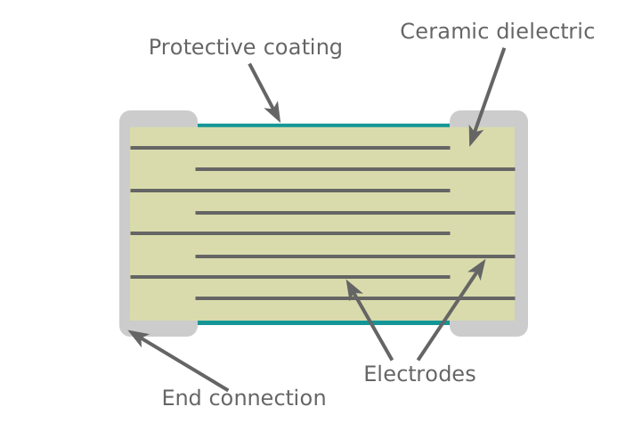
Multilayer Ceramic Capacitors, MLCCs, are used in vast quantities in modern electronics.
Walk into any hardware development lab or slice open a smartphone, and you will find hundreds, if not thousands—of these tiny rectangular blocks filtering noise, decoupling power rails, and stabilizing high-frequency lines.
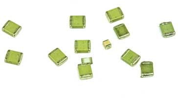
They offer exceptional performance in many ways but contain this within a minute footprint.
However, to get the best from these components it's important to understand their construction and to observe a number of precautions.
Video: Capacitor Secrets: What’s Happening Inside an MLCC MultiLayer Ceramic Capacitor
1. The Voltage Trap: Combating Capacitance Shift
One of the most surprising characteristics of high-capacitance MLCCs is that their capacitance value is not fixed. If you apply a DC voltage across a ceramic capacitor, its effective capacitance will drop—sometimes catastrophically.
In severe cases, some capacitors operating near their rated voltage can exhibit a true capacitance of less than half.
This phenomenon, known as DC bias dependence, occurs primarily in Class II dielectrics (such as X7R, X5R, and Y5V). These materials utilize Barium Titanate (BaTiO3) as their base ceramic.
Barium titanate is a ferroelectric material, meaning its internal crystal domains align spontaneously under an electric field.
When you apply a DC voltage across the capacitor plates, it creates a powerful internal electric field that locks these crystal domains in place.
Because the domains are pinned by the DC voltage, they can no longer freely polarize in response to small AC signals.
Practical Strategies to Minimize DC Bias Shift:
Derate the Voltage Aggressively: The simplest way to combat DC bias shift is to select a capacitor with a rated voltage significantly higher than your operating voltage. If your power rail is 5V, do not use a 6.3V rated capacitor. Opt for a 16V or 25V alternative. Operating an MLCC at 20% to 30% of its maximum voltage rating ensures you retain the vast majority of its nominal capacitance.
Choose Class I Dielectrics for Precision: If your application requires absolute stability (such as timing circuits, filters, or analog signal paths), avoid Class II ceramics entirely. Switch to Class I dielectrics like C0G (also known as NPO). Class I ceramics use non-ferroelectric formulations that exhibit virtually zero capacitance shift with applied voltage, temperature fluctuations, or time. The trade-off is density: C0G capacitors are generally restricted to lower capacitance values (typically under 100 nF in standard packages).
Consult the Manufacturer's Simulation Data: Never rely solely on the headline value printed on the component reel. Before finalizing a BOM, utilize online simulation tools provided by manufacturers—such as Murata's SimSurf or Yageo/Kemet's K-SIM. These tools allow you to input your exact operating DC voltage and temperature to see a graph of the true, expected capacitance.
2. Navigating the Package Size Minefield
As electronics have scaled down, MLCC footprints have shrunk to microscopic proportions. Today, layout designers navigate an array of surface-mount technology (SMT) packages. However, the industry relies on a naming system that contains a massive trap for the unwary.
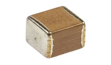
SMD passive components are designated by a four-digit size code. Historically, these codes were established using the EIA Imperial system, where the code represents the component’s length and width in hundredths of an inch. For example, a standard 0805 capacitor measures approximately 0.08 inches long by 0.05 inches wide.
The confusion arises because the international electronics community also uses an EIA Metric system, where the exact same four-digit codes represent dimensions in tenths of a millimetre. Because both systems use four digits, it is incredibly easy to confuse the two standards.
Although the Imperial system is the internationally accepted as the main one and it is the more widely used, but there is considerable room for error.
| Summary of Imperial and Metric SMD Passive Component Codes and Sizes |
||
|---|---|---|
| Imperial Code | Metric Code | Physical Dimensions (Length × Width) |
| 1206 | 3216 | 3.2 mm×1.6 mm |
| 0805 | 2012 | 2.0 mm×1.25 mm |
| 0603 | 1608 | 1.6 mm×0.8 mm |
| 0402 | 1005 | 1.0 mm×0.5 mm |
| 0201 | 0603 | 0.6 mm×0.3 mm |
Note:The 0603 / 0402 Danger Zone: Notice that a Metric 0603 is identical in name to an Imperial 0603, but they represent vastly different physical sizes. Even worse, a Metric 0402 is actually a microscopic Imperial 01005. If a designer places a Metric 0402 footprint on a PCB layout, but the purchasing team orders an Imperial 0402 component, the part will be physically too large for the landing pads, stalling production.
Practical Layout Tips for Size Selection
- Always explicitly state the unit convention on your Bill of Materials (BOM) and schematic notes (e.g., "All SMT footprints are in Imperial codes unless specified"). Furthermore, remember that smaller packages generally exhibit worse DC bias performance for a given capacitance value. If you need a 0.1µF capacitor, an 0805 package will usually retain more capacitance under voltage than an 0402 package because its internal ceramic layers are thicker.
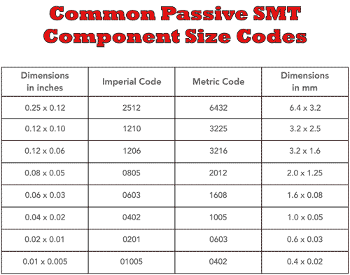
Occasionally for the codes that appear in both imperial and metric lists, for the metric code the letter 'M' is appended to indicate it is metric and reduce confusion.
3. Ceramic cracking and structural integrity
Ceramic materials are exceptionally hard, but they are also incredibly brittle. Unlike tantalum or aluminum electrolytic capacitors, which feature somewhat compliant internal structures, an MLCC is a rigid monolithic block. Coupled with te fact that the components are soldered directly to the board with no leads to take up movement, this makes them highly susceptible to mechanical cracking if the PCB flexes.
Cracking of these capacitors, which is one of the leading causes of catastrophic failures in modern electronics.
When an MLCC cracks, the damage typically takes the form of a 45-degree flexure crack originating near the termination band. If the crack propagates through the alternating internal metal electrodes, it can cause an immediate open circuit.
Worse, over time, moisture and atmospheric contaminants can seep into the micro-fracture, creating a conductive path between the opposing plates. This leads to a localized conductive path and even a short circuit, which can have major effects on the circuit.
Primary Causes of Cracking
PCB Flexure During Assembly: Bending of the circuit board can occur in many ways: snapping panels apart for testing, installing the board into a rigid chassis, or screwing down mounting hardware. It can even occur when the PCB is passed though an infrared reflow machine for solering - as the PCB heats up it can warp causing damage to the capacitors (damage usually occurs as the solder has set and the board cools down).
Thermal Shock: Applying excessive heat directly to the component body with a soldering iron during manual rework, which causes rapid uneven expansion between the ceramic and the metal end-caps.
How to minimize cracking by intelligent layout design
Fortunately, it is possible to drastically reduce the risk of mechanical failure by implementing strategic component placement on your PCB layout.
Ensure components are at 90° relative to bend directon: If the circuit board has a known flexure line. It might be expected that as a result of connector removal, PCB layout, etc there is a more likely plane in which the board will bend, then place the ceramic capacitors at right angles to this. always orient the long axis of the capacitor parallel to the bend line, or 90 degrees relative to the expected maximum bend direction. When the board flexes, a capacitor oriented parallel to the strain will experience far less tensile stress across its ceramic body than one oriented perpendicular to the bend.
Provide Adequate Buffer Zones: Keep large MLCCs (especially sizes 0805, 1206, and larger) away from high-stress areas like screw mounting holes, heavy board-mounted connectors, and panel breakout tabs. A minimum clearance buffer of 3 mm to 5 mm from these features can mean the difference between a reliable board and a latent field failure.
Utilize Flexible Termination MLCCs: For high-reliability applications, select capacitors engineered with a conductive polymer layer embedded within the end terminations (often marketed as "FlexiCap" or "Soft Termination"). This polymer layer acts as a miniature shock absorber, flexing slightly under board strain and preventing the mechanical stress from transferring directly into the brittle ceramic core.
PCB layout design for minimum flexure: Another issue that I have encountered is that of uneven ground planes, etc. Often when designing an RF board, ground planes are required. These may only be required on part of the board, but having only part of the PCB with aground plane can lead to uneven stresses during manufacture, especially in solder reflow. Having a ground plane across the whole board, even if it it not required for part of it will tend to create a more even stress across the board and thereby minimise the bending.
Use capacitors with flexible terminations: Some SMT MLCCs are specially designed to have terminations with some flexibility built in to them. These are often used in high reliability circuits where vibration, etc might lead to cracking and failure. These capacitors have a 'soft-termination' (flex-term) and incorporate a conductive resin/epoxy layer inside the end termination structure itself (between the base electrode and the nickel barrier) to absorb mechanical flex and thermal shock.
4. ESD sensitivity
While engineers routinely worry about static electricity damaging sensitive microcontrollers and semiconductors, they often treat passive components like MLCCs as immune to Electrostatic Discharge (ESD). This is a dangerous misconception. As ceramic capacitors have shrunk to microscopic footprints, they have become highly vulnerable to static damage.
The root cause of this sensitivity lies in the microscopic internal dimensions of the internal layers and their very narrow spacing. To achieve the required capacitance values, manufacturers must stack dozens of alternating metal electrodes separated by ceramic dielectric barriers. Often these are spaced by distances of a few microns, i.e. µm.

To put that in perspective, a human hair is roughly 70µm wide—meaning these internal barriers are up to twenty times thinner than a single strand of hair.
This extreme thinness creates an incredibly volatile relationship with high voltages, dictated by the fundamental physics of electric field intensity:
Where:
E = the electric field strengthin V/m
V is the voltage in V
d is the dielectric thickness in m
as an example, under standard 3.3V or 5V operating conditions, the internal electric field is perfectly safe. However, if an ungrounded human operator or assembly machine touches the circuit board, a static discharge can easily deliver 1,000V to 2,000V to the component. Even walking across a carpet can generate 20kV, although with little charge.
When 1,000V appears across a microscopic 5μm ceramic gap, the calculations yield a terrifying internal electric field of 200 million volts per metre (200 MV/m).
Seeing the figures, it is hardly surprising that this instantly punches right through the dielectric strength of the Barium Titanate ceramic, causing a catastrophic dielectric breakdown.
The static spark literally blasts a physical hole through the micron-thin ceramic barrier, melting the adjacent metal electrodes together. The result is a permanent, latent short circuit that can cause the circuit to fail immediately upon power-up, or worse, degrade over time and fail unpredictably in the field.
Practical Tips to Prevent ESD Damage in MLCCs
Enforce Strict ESD Workstation Standards: Treat MLCCs with the same electrostatic respect you give to fragile ICs. Always handle unpopulated PCBs and component reels while wearing a properly grounded anti-static wrist strap, and work exclusively on dissipative ESD mats.
Select Larger Package Sizes for High-Risk Lines: For decoupling lines that connect directly to the outside world—such as USB data lines, power input jacks, or user-accessible buttons—avoid using ultra-small 0402 or 0201 packages if possible. Opting for a larger 0805 or 1206 package with higher maximum voltage ratings gives the component thicker internal dielectric layers, thereby improving ESD voltage tolerance.
Implement Upstream TVS Protection: Ensure that Transient Voltage Suppressor (TVS) diodes or varistors are placed at the absolute entry point of the PCB interface. These components are designed to clamp the massive 1,000V+ static spike down to a safe level (under 15V) before the pulse ever reaches the fragile, micron-thin layers of your ceramic capacitors.
Implement ESD design practice: Don't just rely on ESD protection diodes, but implement overall good ESD design practice in terms of layout, overall protection and being aware of possible ESD paths, etc.
5. Ceramic capacitor ageing
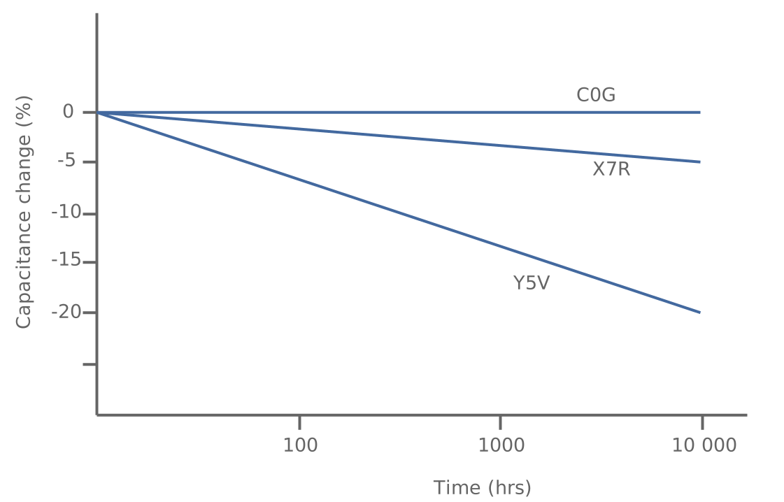
SMT MLCC capacitor aging is a phenomenon that affects Class II ferroelectric ceramics (such as X7R, X5R, and Y5V).
Over time, these capacitors suffer a logarithmic decay in capacitance — a process driven by the gradual relaxation and alignment of the crystal domains within the Barium Titanate (BaTiO3)) structure after initial manufacturing.
The loss in capacitance follows a predictable formula: it decreases by a fixed percentage for every decade of time that passes (e.g., 1 to 10 hours, 10 to 100 hours, 100 to 1,000 hours).
This means the capacitance loss between 1 hour and 10 hours is identical to the loss between 1,000 hours and 10,000 hours (roughly 14 months). The process never truly stops, but it slows dramatically as time goes on.
Crucially, this ageing process is fully reversible through a process called de-aging: heating the capacitor above its Curie temperature (typically around 125° to 150°C) resets the crystal lattice, restoring the component to its full nominal capacitance value.
Design strategies to combat ageing
To manage ceramic capacitor ageing in practical electronic designs, engineers employ a mix of component selection and voltage derating strategies:
Select Class I Dielectrics for Critical Nodes: If a circuit requires long-term parameter stability (such as RF filters, precision timing loops, or analog integrators), avoid Class II ceramics entirely. Class I ceramics like C0G (NPO) do not exhibit ageing effects because they do not utilize ferroelectric materials.
Factor Ageing into Tolerance Calculations: When designing power rail decoupling or bulk storage with X7R or X5R capacitors, explicitly account for the lost capacitance over the product’s expected operating lifetime. For example, a capacitor with a 2.5% aging rate per decade will lose roughly 7.5% of its initial capacitance over 10,000 hours (~1.1 years). Always size the nominal capacitor value higher to ensure it stays above the circuit's minimum threshold after years in the field.
Account for the Soldering Reset: Because reflow soldering temporarily heats the component past its Curie temperature, MLCCs are completely "de-aged" during assembly. Keep in mind that initial factory bench testing will measure the capacitor at its maximum restored value, which will slowly decay down toward its steady-state baseline as the product sits on the shelf or in operation.
Don't spec tight tolerances on Class 2 parts: Specifying a 5% tolerance on an X7R capacitor is counterproductive when natural ageing will drift it past that boundary over time.
Factor in the combo loss: Ageing acts additively alongside DC bias shift and temperature coefficient loss.Always verify final effective capacitance at operational lifetime limits.
6. Microphoney & Piezoelectricity in Class 2 MLCCs
A less widely known characteristic of Class 2 surface-mount ceramic capacitors (such as X7R, X5R, and Y5V) is their susceptibility to piezoelectric behaviour. Class 2 dielectrics rely heavily on Barium Titanate (BaTiO3), a ferroelectric material that possesses inherent piezoelectric properties.
This means the physical structure of the ceramic dielectric mechanical distorts when an electric field is applied across it, and conversely, applying physical stress or vibration to the capacitor generates a small electric charge.
This can be important where the printed circuit board may be subject to vibration, and where the value of the capacitance may have an impact on the circuit characteristics.
Another interesting factor occurs because, when an alternating voltage or ripple current acts across a Class 2 MLCC, the component physically expands and contracts at that frequency. Soldered down onto a printed circuit board, these microscopic mechanical movements transfer directly into the substrate. The PCB essentially acts as a sounding board—much like a loudspeaker cone—translating those microscopic vibrations into an audible hum or squeal known in the industry as "singing capacitors" when the signal falls within the human hearing range (20 Hz to 20 kHz).
Design considerations to mitigate microphonics and acoustic noise
Switch to Class 1 dielectrics if possible for sensitive nodes: Class 1 ceramics like C0G (NP0) do not use ferroelectric materials and are entirely non-piezoelectric. Use C0G capacitors in high-gain analog signal paths, low-noise feedback loops, and frequency-determining circuits.
Utilize low-acoustic / flex-termination MLCCs: For high-capacitance decoupling applications where Class 2 parts are unavoidable, consider specialized MLCC series designed with soft metallic terminations or lead frames. These flexible interfaces mechanically decouple the capacitor body from the PCB substrate, significantly damping acoustic emissions and microphonic pickup.
Optimize component placement and orientation: Placing capacitors back-to-back or staggering their orientation on opposite sides of the PCB can cancel out the mechanical forces applied to the board. Additionally, avoid placing Class 2 decoupling capacitors directly in the center of large, flexible PCB spans, as these regions flex most easily under mechanical vibration.
Conclusion
Ceramic capacitors are indispensable components, but they demand respect at every stage of design from initial schematic simulation to physical PCB layout, manufacture and beyond.
By derating the operating voltages to preserve capacitance, carefully managing imperial and metric package names, and orienting your components to withstand physical board flexing, you can avoid the most common pitfalls of hardware design.
Taking the time to verify these micro-scale parameters ensures any designs remain stable, functional, and reliable for years to come.
 Written by Ian Poole .
Experienced electronics engineer and author.
More Electronic Components:
Batteries
Capacitors
Connectors
ADC
DAC
Diodes
FET
Inductors
Memory types
Phototransistor
Quartz crystals
Relays
Resistors
RF connectors
Switches
Surface mount technology
Thyristor
Transformers
Transistor
Unijunction
Valves / Tubes
Return to Components menu . . .