GaN vs SiC MOSFETs A Design Engineer’s Guide to the Wide Bandgap Revolution
From EV traction inverters to AI data centres, here's a comparison of the performance, thermal ruggedness, and voltage ratings of silicon carbide, SiC and gallium nitride, GaN MOSFETs for modern power design.
Home » Electronic components » this page
FETs, Field Effect Transistors Includes:
FET basics
FET specifications
JFET
MOSFET
Dual gate MOSFET
Power MOSFET
MESFET / GaAs FET
HEMT & PHEMT
FinFET technology
IGBT
IGBT vs MOSFET - which is better?
Silicon carbide, SiC JFET
Silicon carbide, SiC MOSFET
Silicon carbide vs silicon MOSFETs
GaN FET / HEMT
SiC vs GaN
FET component data:
MOSFETs
SiC MOSFETs
GaN FETs
IGBTs
For decades, Silicon, Si, was the undisputed king of the semiconductor world. It was reliable, cheap, and we understood it perfectly.
But as we entered the mid-2020s, our hunger for power grew faster than silicon could handle. Between the "unquenchable thirst" of AI data centres and the global shift toward 800V electric vehicle architectures, a wall was hit. Silicon simply couldn't keep up with the requirements of the modern age.
However, enter the Wide Bandgap (WBG) devices. Both Gallium Nitride, GaN and Silicon Carbide , SiC have moved from "exotic lab materials" to the frontline of power electronics where they are now firmly established.
While SiC MOSFETs and GaN FETs share the Wide Bandgap title, they are as different as a high-speed sports car and a heavy-duty freight truck.
Choosing between them is not just about picking the best technology; instead it’s about picking the right tool for the specific circuit and application.
The Technologies: Lateral Speed vs. Vertical Power
To understand why these materials behave differently, we have to look at their atomic "personality." The term Wide Bandgap refers to the energy required to remove an electron from the valence band to the conduction band.
In Silicon, this gap is about 1.1 eV. In both GaN and SiC, it is roughly 3.2 to 3.4 eV.
While these figures may not mean a lot, in practice it means that these materials to withstand much higher electric fields before breaking down, allowing the devices to be smaller and thinner for the same voltage rating.
GaN: The High Electron Mobility Transistor (HEMT)
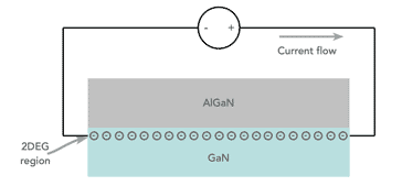
Most commercial Gallium Nitride devices are what are called Lateral HEMTs. Unlike a traditional MOSFET, where current flows vertically through the chip, current in a GaN FET flows across the surface in what is termed a "Two-Dimensional Electron Gas" (2DEG) layer.
This 2DEG layer has incredibly high electron mobility — about 1,500 to 2,000.
Because the electrons move so freely and the device structure is lateral, GaN FETs have almost zero "gate charge" compared to Silicon.
More importantly, they have zero reverse recovery charge.
In a traditional Silicon MOSFET, a "body diode" stores charge that must be cleared out every time the switch turns off, wasting energy. GaN doesn’t have a physical body diode, meaning it can switch on and off millions of times per second (MHz range) without the massive heat buildup that would melt silicon.
SiC: The Vertical MOSFET
Silicon Carbide is a more rugged cousin technology being able to withstand higher voltage, currents and temperatures.
Most SiC devices have a Vertical format for the MOSFETs. Current flows from the top of the die down to the bottom. This architecture is much better at handling raw power and high voltages.
While electron mobility within silicon carbide is lower than gallium nitride its thermal conductivity is considerably better.
SiC has a thermal conductivity of 490 W/m·K, which is nearly three times that of Silicon and significantly higher than that of gallium nitride at 130 W/m·K.
This means that even though SiC might generate some heat during switching, it is much better at removing the heat from the chip and into the heatsink.
Performance Differences: Speed vs. Stamina
When comparing performance, the main areas for comparison are the switching loss, thermal management and the maximum voltage rating.
• Speed & switching loss
For high frequency switching GaN is a very clear winner. Because GaN FETs have much lower parasitic capacitances, they can transition between the "on" and "off" states in nanoseconds.
This is critical because most energy in a power supply is lost during that tiny window of time when the device is switching. It is when the device is between the on and of states that resistive losses occur.
By switching faster, GaN reduces the switching losses by up to 80% compared to Silicon and significantly outperforms SiC in applications above 100 kHz.
GaN-based power supplies currently operating comfortably in the 1 MHz to 10 MHz range, allowing designers to use much smaller inductors and capacitors that would have been impossible a decade ago.
• Heat & thermal ruggedness
Here there is a dilemma. GaN is faster, but SiC can be said to be tougher. In high-power applications (kilowatts to megawatts), devices inevitably get hot. silicon carbide is able to survive these environments much better.
A SiC MOSFET can operate at junction temperatures exceeding 200°C without losing its breakdown voltage capability.
Furthermore, because the on resistance of SiC increases more slowly with temperature than does silicon, silicon carbide remains efficient even when pushed to its limits.
In a heavy industrial motor drive or a locomotive inverter, where cooling is a constant challenge, ability of silicon carbide to perform well at temperature makes it the preferred choice.
• Maximum voltage
Current technology is seeing a divide between silicon carbide and gallium nitride.
GaN applications: Generally dominates the 100V to 650V range. While 1,200V GaN devices are now sampling in 2026, they are still specialized.
SiC Territory: Dominates the 650V to 1,700V+ range. If you are working with an 800V EV battery or a 1,500V solar array, SiC is the undisputed champion.
Where Should Each Technology Be Used?
Choosing between GaN and SiC isn't just about the device itself, the decision revolves around the overall system.
• Where GaN Wins: Density and Portability
GaN is the go-to for anything that needs to be small, light, and efficient. It tends not to be used inth e applicatiosn where high temeprature and rough and rugged oeprationa re needed.
Consumer Fast Chargers: This was GaN's first big win. You can now get a 100W laptop charger that fits in your pocket because GaN’s high switching frequency allows for a 70% reduction in the size of the transformer.
AI Data Centres: In 2026, data centres are shifting to 48V DC power distribution. GaN is perfect for the DC-DC converters that sit right next to the high-power GPUs, providing 99% efficiency in a tiny footprint.
LiDAR for Autonomous Vehicles: LiDAR requires incredibly fast, high-current pulses of light to "see" the surroundings. GaN’s nanosecond switching speed is the only technology that can drive these lasers with the precision required for Level 4 autonomy.
• Where SiC Wins: Raw Power and Reliability
SiC is the backbone of the heavy-duty green energy revolution. It is widely used in many power applicatiosn where current levels are high and where temperatures can rise.
EV Traction Inverters: This is the "killer app" for SiC. By replacing Silicon IGBTs with SiC MOSFETs in the main motor controller, EV manufacturers can increase range by 5% to 10% simply by reducing energy waste.
Solar & Wind Grid Inverters: When converting DC power from a massive solar farm into AC for the grid, you are dealing with thousands of volts and hundreds of amps. SiC’s high voltage rating and thermal conductivity allow these inverters to be smaller and more reliable, reducing the "Levelized Cost of Energy" (LCOE).
Industrial Motor Drives: In factories, motors run 24/7. The efficiency gains from SiC mean less wasted electricity and longer intervals between maintenance, as the cooling systems don't have to work as hard.
Design considerations
It's not possible to drop a GaN or SiC FET into a board designed for Silicon. These devices are very sensitive to circuit layout and other circuit considerations.
Because GaN switches so fast (up to 150 V/ns), even a few millimeters of extra trace length can create parasitic inductance that leads to massive voltage rings and EMI (electromagnetic interference).
Engineers are increasingly moving toward Integrated GaN (GaNFast) solutions, where the gate driver and the power transistor are on the same piece of silicon to minimize these loops.
SiC is slightly more forgiving but requires a much higher Gate Drive Voltage. While a Silicon MOSFET might turn on with 10V, a SiC MOSFET often needs +18V to +20V to fully open the "channel" and reach its lowest resistance, and it often needs a negative voltage (-3V to -5V) to ensure it stays off during high-speed transitions.
Best application areas
The "GaN vs. SiC" debate is no longer a war — it’s a partnership. It is no longer an era of trying to make one material or device type do everything. Each type has its own areas where it is best suited.
Choose Gallium Nitride (GaN): if your priority is size, frequency, and mid-range voltage. If it needs to be "ultra-compact" or "ultra-fast," GaN is your answer.
Choose Silicon Carbide (SiC): if your priority is thermal performance, high voltage, and raw power handling. If it’s going in a vehicle, a train, or a power grid, SiC is the king.
As we look toward the end of the 2020s, the only real loser in this battle is the traditional Silicon MOSFET in high-performance applications. While Silicon will always have a home in low-cost, low-power gadgets, the future of the global energy grid and our digital world is is increasingly being built on the wide band gap materisl, GaN and SiC.
Summary of Key Highlight Facts
Bandgap Strength: SiC and GaN have a bandgap ~3x wider than Silicon, allowing for 10x higher breakdown fields.
Electron Mobility: GaN leads with ~2,000 , enabling MHz switching speeds.
Thermal Conductivity: SiC leads with **490 W/m·K**, roughly 3.7x higher than GaN and 3.2x higher than Silicon.
Efficiency Gains: Replacing Silicon with SiC in an EV traction inverter can increase vehicle range by **5–10%**.
System Size: GaN can shrink power adapters and DC-DC converters by **up to 70%** by allowing for smaller passive components (inductors/capacitors).
Current Trend: The industry is transitioning to 200mm SiC wafers and 300mm GaN-on-Si wafers to drive down costs.
Voltage Sweet Spots: GaN dominates > 650V; SiC dominates 650V – 3,300V+.
Reverse Recovery: GaN has zero, making it the cleanest switcher for high-frequency bridge topologies.
 Written by Ian Poole .
Experienced electronics engineer and author.
More Electronic Components:
Batteries
Capacitors
Connectors
ADC
DAC
Diodes
FET
Inductors
Memory types
Phototransistor
Quartz crystals
Relays
Resistors
RF connectors
Switches
Surface mount technology
Thyristor
Transformers
Transistor
Unijunction
Valves / Tubes
Return to Components menu . . .